
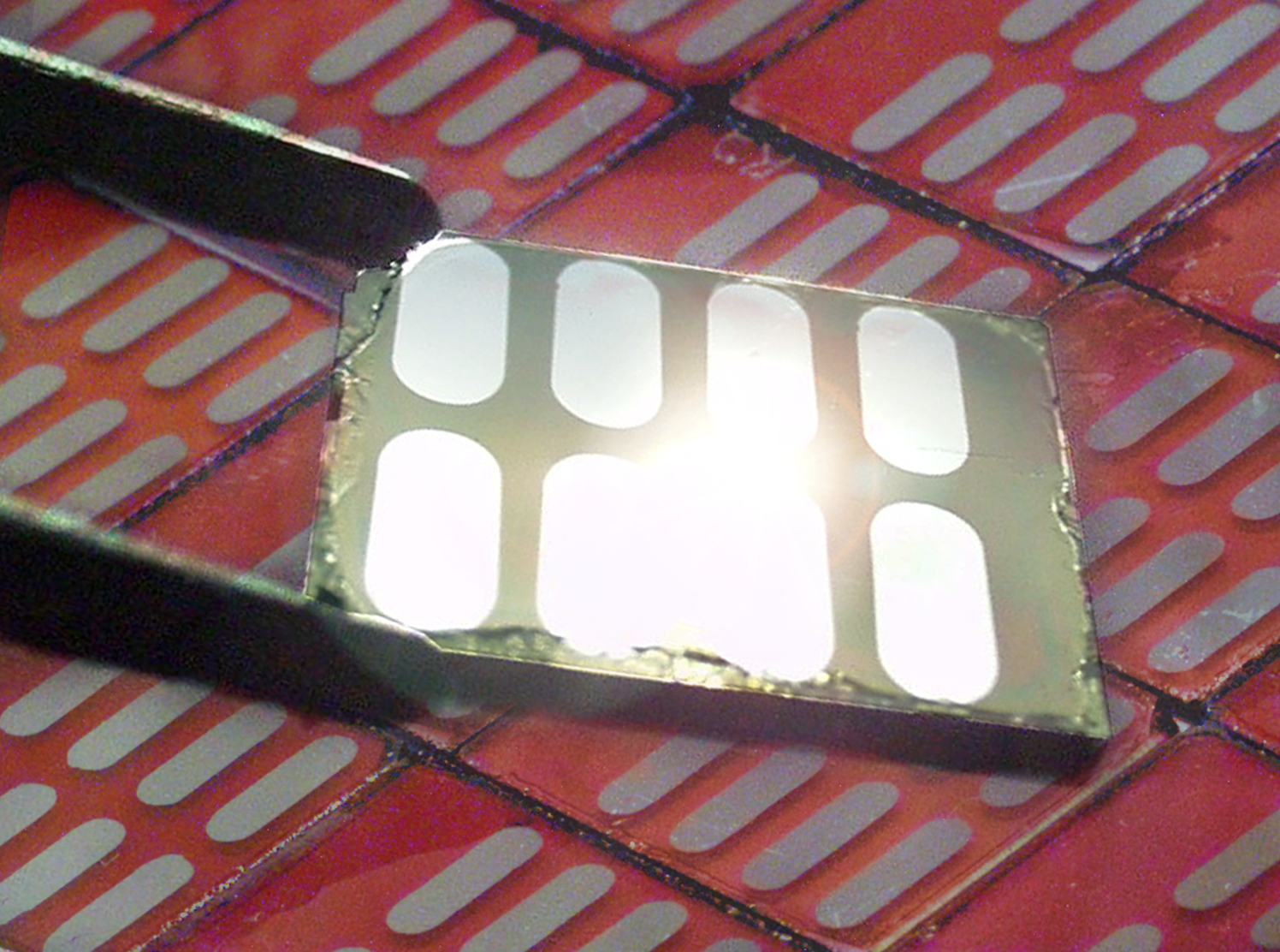
A new and better way to study “hot” carriers in semiconductors, a major source of efficiency loss in solar cells, has been developed by scientists at Berkeley Lab. (Photo by Roy Kaltschmidt)
One of the major road blocks to the design and development of new, more efficient solar cells may have been cleared. Researchers with the Lawrence Berkeley National Laboratory (Berkeley Lab) have developed the first ab initio method – meaning a theoretical model free of adjustable or empirical parameters – for characterizing the properties of “hot carriers” in semiconductors. Hot carriers are electrical charge carriers – electrons and holes – with significantly higher energy than charge carriers at thermal equilibrium.
“Hot carrier thermalization is a major source of efficiency loss in solar cells, but because of the sub-picosecond time scale and complex physics involved, characterization of hot carriers has long been a challenge even for the simplest materials,” says Steven Louie, a theoretical physicist and senior faculty scientist with Berkeley Lab’s Materials Sciences Division (MSD). “Our work is the first ab initio calculation of the key quantities of interest for hot carriers – lifetime, which tells us how long it takes for hot carriers to lose energy, and the mean free path, which tells us how far the hot carriers can travel before losing their energy.”
All previous theoretical methods for computing these values required empirical parameters extracted from transport or optical measurements of high quality samples, a requirement that among the notable semiconductor materials has only been achieved for silicon and gallium arsenide. The ab initio method developed by Louie and Jeff Neaton, Director of the Molecular Foundry, a U.S. Department of Energy (DOE) Nanoscience User Facility hosted at Berkeley Lab, working with Marco Bernardi, Derek Vigil-Fowler and Johannes Lischner, requires no experimental parameters other than the structure of the material.
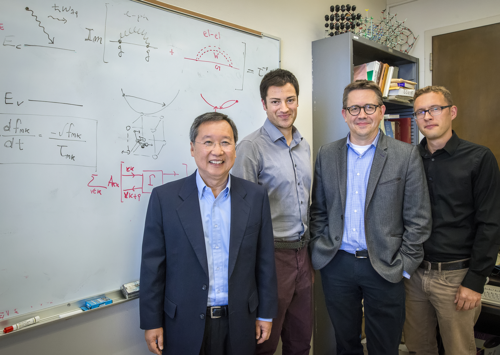
(From left) Steve Louie, Marco Bernardi, Jeff Neaton and Johannes Lischner developed the first ab initio method for characterizing hot carriers in semiconductors. (Photo by Roy Kaltschmidt)
“This means that we can study hot carriers in a variety of surfaces, nanostructures, and materials, such as inorganic and organic crystals, without relying on existing experiments,” says Neaton. “We can even study materials that have not yet been synthesized. Since we can access structures that are ideal and defect-free with our methods, we can predict intrinsic lifetimes and mean free paths that are hard to extract from experiments due to the presence of impurities and defects in real samples. We can also use our model to directly evaluate the influence of defects and impurities.”
Neaton, like Louie, is a senior MSD faculty scientist with the University of California (UC) Berkeley. Neaton also holds an appointment with the Kavli Energy NanoSciences Institute. They are the corresponding authors of a paper in Physical Review Letters describing this work titled “Ab Initio Study of Hot Carriers in the First Picosecond after Sunlight Absorption in Silicon.” Bernardi is the lead author of the paper, and Vigil-Fowler the primary coauthor.
Single-junction solar cells based on crystalline silicon are rapidly approaching the theoretical limit of their efficiency, which is approximately 30-percent. This means that if a silicon-based solar cell collects 1,000 Watts per square meter of energy, the most electricity it can generate is 300 Watts per square meter. Hot carriers are crucial to enhancing solar cell efficiency, since their thermalization results in the loss of as much as a third of the absorbed solar energy in silicon, and similar values in other semiconductors. However, the properties of hot carriers in complex materials for photovoltaic and other modern optoelectronic applications are still poorly understood.
“Our study was aimed at providing useful data for hot carrier dynamics in silicon with application in solar cells,” says Bernardi. “In this study we provide calculations from first principles that describe the two key loss mechanisms, induced by electrons and phonons, respectively, with state-of-the-art accuracy and within the frameworks of density functional and many-body perturbation theories.”
When the research team applied their method to study the relaxation time and mean free path of hot carriers in silicon, they found that thermalization under solar illumination is completed within 350 femtoseconds, and is dominated by phonon emission from hot carriers, a process that becomes progressively slower as the hot carriers lose energy and relax toward the band edges. This modeling result was in excellent agreement with the results of pump-probe experiments. While the model was only tested on silicon in this study, the researchers are confident it will be equally successful with other materials.
“We believe our approach is highly valuable to experimental groups studying hot carriers in the context of solar cells and other renewable energy technologies as it can be used to compute the lifetime and mean free path of hot carriers with specific energies, momenta, and crystallographic directions with unprecedented resolution,” Bernardi says. “As we expand our study of hot carriers to a range of crystalline materials and nanostructures, we believe that our data will provide unique microscopic insight to guide new experiments on hot carriers in semiconductors.”
This research was supported by the DOE Office of Science and the National Science Foundation and made use of the Molecular Foundry, as well as computational resources of the National Energy Research Scientific Computing Center (NERSC), which is also supported by the DOE Office of Science.
Additional Information
For more about the research of Steven Louie go here
For more about the research of Jeff Neaton go here
For more about the Molecular Foundry go here
For more about NERSC go here
For more about the Kavli Energy NanoSciences Institute go here