
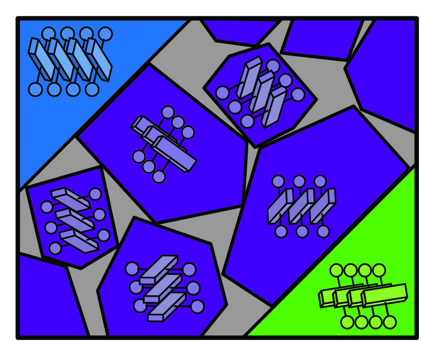
Sketch of organic semiconductor thin film shows that the interfacial region between larger domains (blue and green) consists of randomly oriented small, nano-crystalline domains (purple).
Organic semiconductors are prized for light emitting diodes (LEDs), field effect transistors (FETs) and photovoltaic cells. As they can be printed from solution, they provide a highly scalable, cost-effective alternative to silicon-based devices. Uneven performances, however, have been a persistent problem. Scientists have known that the performance issues originate in the domain interfaces within organic semiconductor thin films, but have not known the cause. This mystery now appears to have been solved.
Naomi Ginsberg, a faculty chemist with the U.S. Department of Energy (DOE)’s Lawrence Berkeley National Laboratory and the University of California (UC) Berkeley, led a team that used a unique form of microscopy to study the domain interfaces within an especially high-performing solution-processed organic semiconductor called TIPS-pentacene. She and her team discovered a cluttered jumble of randomly oriented nanocrystallites that become kinetically trapped in the interfaces during solution casting. Like debris on a highway, these nanocrystallites impede the flow of charge-carriers.
“If the interfaces were neat and clean, they wouldn’t have such a large impact on performance, but the presence of the nanocrystallites reduces charge-carrier mobility,” Ginsberg says. “Our nanocrystallite model for the interface, which is consistent with observations, provides critical information that can be used to correlate solution-processing methods to optimal device performances.”

Naomi Ginsberg (forefront) led a team consisting of (from left) Cathy Wong, Benjamin Cotts and Hao Wu that identified nanocrystallites in domain interfaces as the mysterious source of performance issues in organic semiconductors. (Photo by Kelly Owen)
Ginsberg, who holds appointments with Berkeley Lab’s Physical Biosciences Division and its Materials Sciences Division, as well as UC Berkeley’s departments of chemistry and physics and is a member of the Kavli Energy NanoScience Institute at Berkeley, is the corresponding author of a paper describing this research in Nature Communications. The paper is titled “Exciton dynamics reveals aggregates with intermolecular order at hidden interfaces in solution-cast organic semiconducting films.” Co-authors are Cathy Wong, Benjamin Cotts and Hao Wu.
Organic semiconductors are based on the ability of carbon to form larger molecules, such as benzene and pentacene, featuring electrical conductivity that falls somewhere between insulators and metals. Through solution-processing, organic materials can usually be fashioned into crystalline films without the expensive high-temperature annealing process required for silicon and other inorganic semiconductors. However, even though it has long been clear that the crystalline domain interfaces within semiconductor organic thin films are critical to their performance in devices, detailed information on the morphology of these interfaces has been missing until now.
“Interface domains in organic semiconductor thin films are smaller than the diffraction limit, hidden from surface probe techniques such as atomic force microscopy, and their nanoscale heterogeneity is not typically resolved using X-ray methods,” Ginsberg says. “Furthermore, the crystalline TIPS-pentacene we studied has virtually zero emission, which means it can’t be studied with photoluminescence microscopy.”
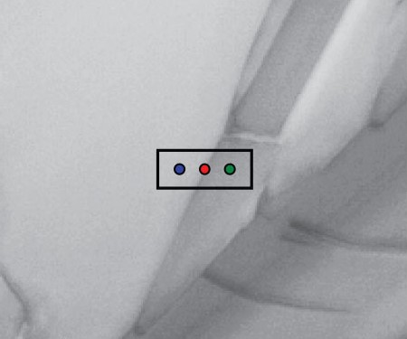
Wide field polarized transmission image of TIPS-pentane film with region-of-interest highlighted. The colored spots mark the location of TA microscopy measurements. (Image courtesy of Naomi Ginsberg)
Ginsberg and her group overcame the challenges by using transient absorption (TA) microscopy, a technique in which femtosecond laser pulses excite transient energy states and detectors measure the changes in the absorption spectra. The Berkeley researchers carried out TA microscopy on an optical microscope they constructed themselves that enabled them to generate focal volumes that are a thousand times smaller than is typical for conventional TA microscopes. They also deployed multiple different light polarizations that allowed them to isolate interface signals not seen in either of the adjacent domains.
“Instrumentation, including very good detectors, the painstaking collection of data to ensure good signal-to-noise ratios, and the way we crafted the experiment and analysis were all critical to our success,” Ginsberg says. “Our spatial resolution and light polarization sensitivity were also essential to be able to unequivocally see a signature of the interface that was not swamped by the bulk, which contributes much more to the raw signal by volume.”
The methology developed by Ginsberg and her team to uncover structural motifs at hidden interfaces in organic semiconductor thin films should add a predictive factor to scalable and affordable solution-processing of these materials. This predictive capability should help minimize discontinuities and maximize charge-carrier mobility. Currently, researchers use what is essentially a trial-and-error approach, in which different solution casting conditions are tested to see how well the resulting devices perform.
“Our methodology provides an important intermediary in the feedback loop of device optimization by characterizing the microscopic details of the films that go into the devices, and by inferring how the solution casting could have created the structures at the interfaces,” Ginsberg says. “As a result, we can suggest how to alter the delicate balance of solution casting parameters to make more functional films.”
This research was primarily funded by the Defense Advanced Research Projects Agency.
Additional Information
For more about the research of Naomi Ginsberg and her group go here
# # #
Lawrence Berkeley National Laboratory addresses the world’s most urgent scientific challenges by advancing sustainable energy, protecting human health, creating new materials, and revealing the origin and fate of the universe. Founded in 1931, Berkeley Lab’s scientific expertise has been recognized with 13 Nobel prizes. The University of California manages Berkeley Lab for the U.S. Department of Energy’s Office of Science. For more, visit www.lbl.gov.
DOE’s Office of Science is the single largest supporter of basic research in the physical sciences in the United States, and is working to address some of the most pressing challenges of our time. For more information, please visit the Office of Science website at science.energy.gov/.