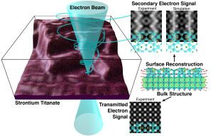
A highly promising technique called “high-resolution scanning electron microscopy,” or HRSEM, extends scanning microscopy to the atomic scale and provides information on both surface and bulk atoms simultaneously.
For the first time in the long and vaunted history of scanning electron microscopy, the unique atomic structure at the surface of a material has been resolved. This landmark in scientific imaging was made possible by a new analytic technique developed by a multi-institutional team of researchers, including scientists from the U.S. Department of Energy (DOE)’s Lawrence Berkeley National Laboratory (Berkeley Lab).
“We’ve developed a reasonably direct method for determining the atomic structure of a surface that also addresses the very challenging problem of buried interfaces,” says Jim Ciston, a staff scientist with the National Center for Electron Microscopy (NCEM) at the Molecular Foundry, a DOE Office of Science User Facility. “Although surface atoms represent a minuscule fraction of the total number of atoms in a material, these atoms drive a large portion of the material’s chemical interactions with its environment.”
Ciston is the lead and corresponding author of a paper describing this new analytical method in the journal Nature Communications. The article is titled “Surface Determination through Atomically Resolved Secondary Electron Imaging.” Other co-authors are Hamish Brown, Adrian D’Alfonso, Pratik Koirala, Colin Ophus, Yuyuan Lin, Yuya Suzuki, Hiromi Inada, Yimei Zhu, Les Allen, and Laurence Marks.
Most materials interact with other materials through their surfaces, which are often different in both structure and chemistry from the bulk of the material. Many important processes take place at surfaces, ranging from the catalysts used for the generation of energy-dense fuels from sunlight and carbon dioxide, to how bridges and airplanes rust.

Jim Ciston and Colin Ophus at Berkeley Lab’s TEAM 1.0, the world’s most powerful electron microscope. (Photo by Roy Kaltschmidt)
“In essence, the surface of every material can act as its own nanomaterial coating that can greatly change its chemistry and behavior,” Ciston says. “To understand these processes and improve material performance it is vital to know how the atoms are arranged at surfaces. While there are now many good methods for obtaining this information for rather flat surfaces, when the surfaces are rough most currently available tools are limited in what they can reveal.”
“The beauty of this technique is that we can image surface atoms and bulk atoms simultaneously,” says co-author Zhu, a scientist at Brookhaven National Laboratory. “Currently none of any existing methods can achieve this.”
Scanning electron microscopy (SEM) is an excellent technique for studying surfaces but typically provides information only about topology at nanoscale resolution. A highly promising new version of scanning electron microscopy, called “high-resolution scanning electron microscopy,” or HRSEM, extends this resolution to the atomic scale and provides information on both surface and bulk atoms simultaneously, retaining much of the surface sensitivity of traditional SEM through secondary electrons.
Secondary electrons are the result of a highly energized beam of electrons striking a material and causing atoms in the material to emit energy in the form of electrons rather than photons. As a large portion of secondary electrons are emitted from the surface of a material in addition to its bulk they are good resources for obtaining information about atomic surface structure. However, the surface selectivity of HRSEM has never been fully exploited.
“Even though powerful instruments have been available for several years, progress in materials science applications has been slow due to an inability to directly interpret the surface and bulk components of HRSEM images independently,” Ciston says. “This difficulty stemmed from the lack of a fully-developed theoretical framework to understand SEM image formation at the atomic scale.”

Surface atoms represent a tiny fraction of the total number of atoms in a material but drive a large portion of the material’s chemical interactions with its environment.
Existing secondary electron image simulation methods had to be extended to take into account contributions from valence orbitals in the material, he says, and also the effect of dielectric screening on the efficiency of generating signal from those valence orbitals.
To verify the effectiveness of their new theoretical framework, Ciston, Allen, Marks and their colleagues collected and analyzed in detail a series of HRSEM images of a particular arrangement of atoms at the surface of strontium titanate. These experiments were coupled with careful secondary electron image simulations, density functional theory calculations, and aberration-corrected high resolution transmission electron microscopy.
“Conventional transmission electron microscopy images are well-understood and were needed to confirm that we actually had the correct structure and that the new HRSEM theory was on the right track,” Ciston says. “Taken collectively, the analysis enabled us to unambiguously reference surface information to information from the bulk crystal.”
The excellent agreement between calculations and experimental results showed that HRSEM is a highly promising tool for surface structure determination, including the challenging topic of bulk/surface registration. From their demonstration, the collaboration discovered that previously reported atomic surface structures for strontium titanate with a “6×2 periodicity” are wrong, having failed to detect an unusual seven-fold coordination within a typically high surface coverage of titanium oxide groups.
“We started this work by investigating a well-studied material, but new technique is so powerful that we had to revise much of was already thought to be well-known,” Ciston says.
Co-author Allen, a scientist with Melbourne University in Australia, who led the theoretical and modeling aspects of the new imaging technique, adds: “we now have a sophisticated understanding of what the images mean”.
Perhaps the first target for applying this new HRSEM surface analytic technique will be the study of surface structures on the facets of nanoparticles. The surface structures of nanoparticle facets are extremely challenging to image in the plan view (seen from above) using electron microscopy, a deficit that needs to be corrected as Ciston explains.
“Plan view geometry is important because surface structures will often develop multiple domains, and we need to be sure we’re not projecting through multiple structures and orientations,” he says. “This is a very challenging problem since scanning probe techniques cannot usually address nanoparticle surfaces at atomic resolution, and surface X-ray diffraction requires large, single crystal surfaces.”
Says co-author Marks, a professor of materials science and engineering at Northwestern University, “We are also quite excited by the possibilities of applying these to corrosion problems. The cost to industry and the military of corrosion is enormous, and we need to understand everything that is taking place to produce materials which will last longer.”
This research was primarily funded by the DOE Office of Science.
Additional Information
For more about Berkeley Lab’s Molecular Foundry go here
# # #
Lawrence Berkeley National Laboratory addresses the world’s most urgent scientific challenges by advancing sustainable energy, protecting human health, creating new materials, and revealing the origin and fate of the universe. Founded in 1931, Berkeley Lab’s scientific expertise has been recognized with 13 Nobel prizes. The University of California manages Berkeley Lab for the U.S. Department of Energy’s Office of Science. For more, visit www.lbl.gov.
DOE’s Office of Science is the single largest supporter of basic research in the physical sciences in the United States, and is working to address some of the most pressing challenges of our time. For more information, please visit the Office of Science website at science.energy.gov/.
