
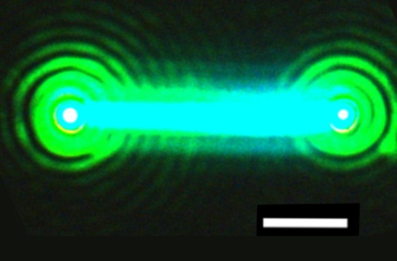
This nanowire, composed of cesium, lead and bromide (CsPbBr3), emits bright laser light after hit by a pulse from another laser source. The nanowire laser proved to be very stable, emitting laser light for over an hour. It also was demonstrated to be broadly tunable across green and blue wavelengths. The white line is a scale bar that measures 2 microns, or millionths of an inch. (Credit: Sam Eaton/UC Berkeley)
Scientists at the U.S. Department of Energy’s Lawrence Berkeley National Laboratory (Berkeley Lab) and UC Berkeley have found a simple new way to produce nanoscale wires that can serve as tiny, tunable lasers.
The nanowires, with diameters as small as 200 nanometers (billionths of a meter) and a blend of materials that has also proven effective in next-generation solar cell designs, were shown to produce very bright, stable laser light. Researchers say the excellent performance of these tiny lasers is promising for the field of optoelectronics, which is focused on combining electronics and light to transmit data, among other applications.
Light can carry far more data, far more rapidly than standard electronics—a single fiber in a fiber-optic cable, measuring less than a hair’s width in diameter, can carry tens of thousands of telephone conversations at once, for example. And miniaturizing lasers to the nanoscale could further revolutionize computing by bringing light-speed data transmission to desktop and ultimately handheld computing devices.
“What’s amazing is the simplicity of the chemistry here,” said Peidong Yang, a chemist in Berkeley Lab’s Materials Sciences Division who led the research, published Feb. 9 in Proceedings of the National Academy of Sciences. More standard techniques that produce nanowires can require expensive equipment and exotic conditions, such as high temperatures, and can suffer from other shortcomings.
The research team developed a simple chemical-dipping solution process to produce a self-assembled blend of nanoscale crystals, plates and wires composed of cesium, lead and bromine (with the chemical formula: CsPbBr3). The same chemical blend, with a molecular architecture composed of cube-like crystal structures, has also proven effective in an emerging wave of new designs for high-efficiency solar cells.
“Most of the earlier work with these types of materials is focused on these solar energy applications,” said Yang, who also holds appointments with UC Berkeley and the Kavli Energy NanoScience Institute at Berkeley Lab and UC Berkeley. “There has been so much progress with these materials in just the past several years—I have a feeling these materials will open a new research frontier for optoelectronics as well,” he said, and in the broader field of photonics, which is focused on using light for a range of applications.
“The whole purpose of developing nano-sized lasers is to interface photonic (light-based) devices with electronic devices seamlessly,” Yang said, “at scales relevant to today’s computer chips. Today, these photonic devices can be bulky.”
Yang’s research team pioneered the development of nanowire lasers almost 15 years ago using a different blend of materials, including zinc oxide (ZnO) and gallium nitride (GaN). But these and other, more conventional combinations of materials used to make nanolasers have shortcomings that can include limited tunability, low brightness or costly manufacturing processes.
In this latest work, the research team discovered how to produce nanowires by dipping a thin lead-containing film into a methanol solution containing cesium, bromine and chlorine heated to about 122 degrees Fahrenheit. A mix of cesium lead bromide crystalline structures formed, including nanowires with a diameter from 200 to 2,300 nanometers (0.2 to 2.3 microns) and a length ranging from 2 to 40 microns.
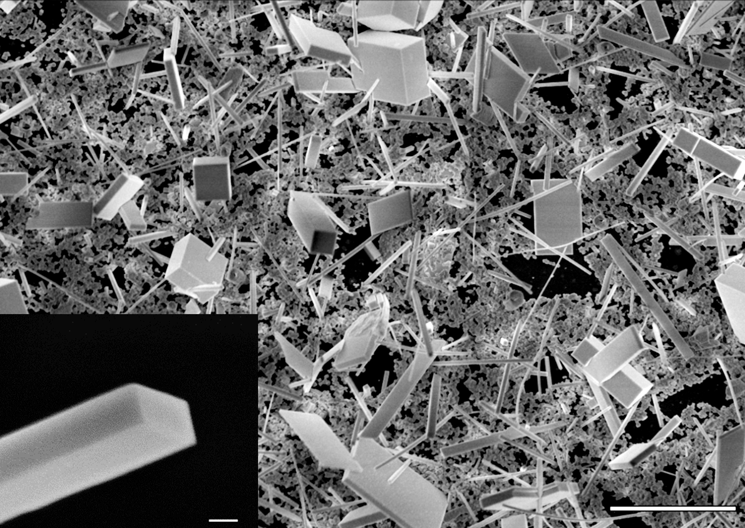
A nanowire construction zone: This scanning electron microscope image shows a collection of cesium lead bromide (CsPgbBr3) nanowires and nanoplates grown from a chemical-dipping process. To produce these structures, researchers dipped a thin lead-containing film into a methanol solution containing cesium, bromine and chlorine heated to about 122 degrees. The white scale bar at the lower right represents 10 microns. The image at the bottom left shows the well-formed rectangular end of a nanowire—the white scale bar associated with it represents 500 nanometers. (Credit: Sam Eaton/UC Berkeley)
Select nanowires used in the experiment were placed on a quartz base and excited by another laser source that caused them to emit light. Researchers found that the nanowire lasers emitted light for over 1 billion cycles after being hit by an ultrafast pulse of visible, violet light that lasted just hundredths of quadrillionths of seconds, which Yang said demonstrated remarkable stability.
Yang said to his knowledge these nanowires may be the first to emit laser light using a totally inorganic (not containing carbon) blend of materials. Researchers demonstrated that the nanowire lasers could be tuned to a range of light including visible green and blue wavelengths.
The nanowires have a crystal structure that resembles that of a naturally occurring mineral known as perovskite. Researchers studied their structure with a technique known as transmission electron microscopy at the National Center for Electron Microscopy, part of Berkeley Lab’s Molecular Foundry. The Molecular Foundry is a DOE Office of Science User Facility.
The nanowires’ crystalline structure is a lot like salt, which does make them susceptible to damage from moisture in the air, Yang said.
“That is one weakness—something we have to study and understand how to improve,” he said. It may be possible to coat the nanowires with polymers or other material to make them more damage-resistant, he said. There are also opportunities to test out other materials and learn whether they improve performance, he said, such as substituting tin for lead.
Ted Sargent, a nanotechnology researcher and professor at University of Toronto who is familiar with the study, said, “The results indicate significant promise for perovskite nanomaterials in lasing.” Also, he said, the stability of the nanolasers, which were shown to operate in air for more than an hour, was “impressive.”
Yang said, “This field is rapidly evolving. We just jumped into this field only 12 months ago, and these lasers are already amazing, bright emitters. It’s just so exciting.”
The work was supported by the DOE Office of Science, the Camille and Henry Dreyfus Foundation, and Suzhou Industrial Park. DOE Office of Science support came partly through the Joint Center for Artificial Photosynthesis, a DOE Energy Innovation Hub led by the California Institute of Technology in partnership with Berkeley Lab.
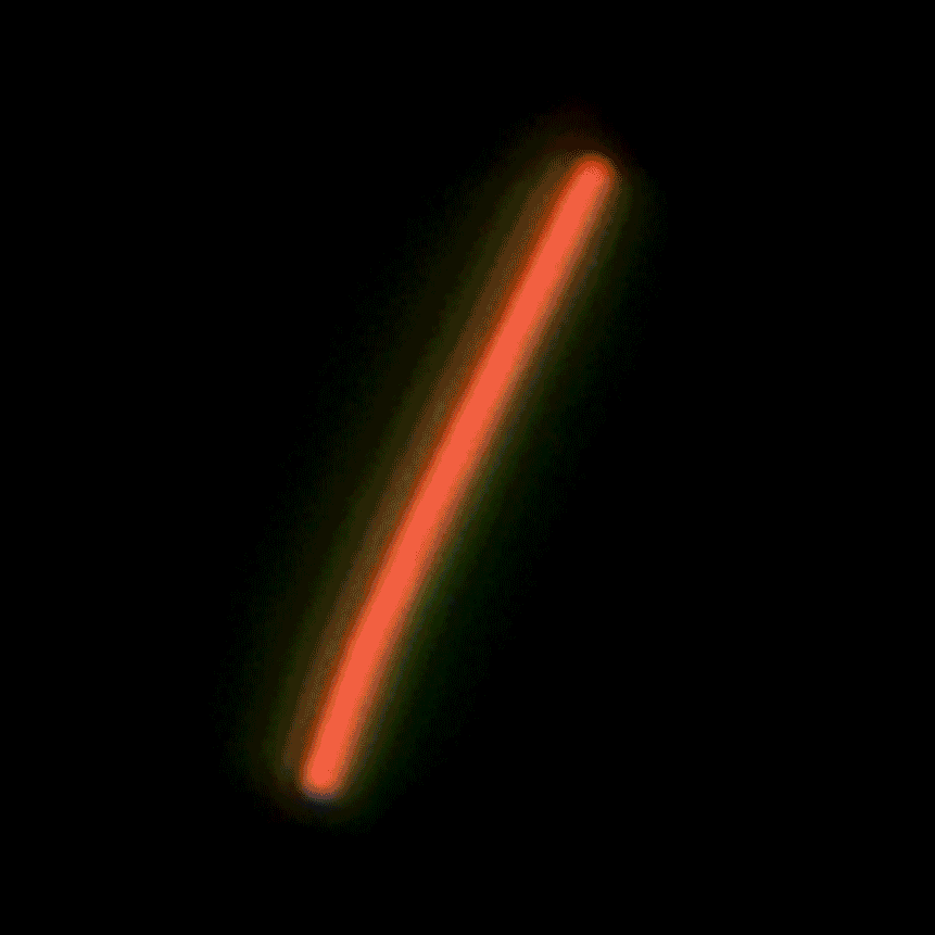
This sequence of nanolaser images shows a dark-field image of a cesium lead bromide nanowire (red) that emits increasingly bright laser light (green) when excited by an external laser. (Credit: Sam Eaton/UC Berkeley)
###
Lawrence Berkeley National Laboratory addresses the world’s most urgent scientific challenges by advancing sustainable energy, protecting human health, creating new materials, and revealing the origin and fate of the universe. Founded in 1931, Berkeley Lab’s scientific expertise has been recognized with 13 Nobel prizes. The University of California manages Berkeley Lab for the U.S. Department of Energy’s Office of Science. For more, visit www.lbl.gov.
The DOE Office of Science is the single largest supporter of basic research in the physical sciences in the United States and is working to address some of the most pressing challenges of our time. For more information, please visit science.energy.gov.
For more information about Peidong Yang’s research, visit: http://nanowires.berkeley.edu/.