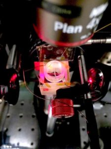
This photo shows the setup for a system known as CAGE (Critically coupled waveguide-Amplified Graphene Electric field imaging device) that is designed to precisely record the properties of faint electrical signals using an infrared laser and a layer of graphene. The CAGE platform can be used to image the electrical signals of living cells. (Credit: Halleh Balch and Jason Horng/Berkeley Lab and UC Berkeley)
Scientists have enlisted the exotic properties of graphene, a one-atom-thick layer of carbon, to function like the film of an incredibly sensitive camera system in visually mapping tiny electric fields in a liquid. Researchers hope the new method will allow more extensive and precise imaging of the electrical signaling networks in our hearts and brains.
The ability to visually depict the strength and motion of very faint electrical fields could also aid in the development of so-called lab-on-a-chip devices that use very small quantities of fluids on a microchip-like platform to diagnose disease or aid in drug development, for example, or that automate a range of other biological and chemical analyses.
The setup could potentially be adapted for sensing or trapping specific chemicals, too, and for studies of light-based electronics (a field known as optoelectronics).
A new way to visualize electric fields
“This was a completely new, innovative idea that graphene could be used as a material to sense electrical fields in a liquid,” said Jason Horng, a co-lead author of a study published Dec. 16 in Nature Communications that details the first demonstration of this graphene-based imaging system. Horng is affiliated with the Kavli Energy NanoSciences Institute, a joint institute at Lawrence Berkeley National Laboratory (Berkeley Lab) and UC Berkeley, and is a postdoctoral researcher at UC Berkeley.
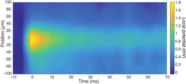
This chart, produced using imaging data from the CAGE system, maps out a tiny electrical field in a fluid as the field dissipates over time. The strength of the field is color-coded, with yellow showing its peak and dark blue showing the weakest field strength. This chart covers the first 70 milliseconds (thousandths of a second) after the field is generated, and the area covered by the field is represented in microns, or millionths of a meter. (Credit: Halleh Balch and Jason Horng/Berkeley Lab and UC Berkeley)
The idea sprang from a conversation between Feng Wang, a faculty scientist in Berkeley Lab’s Materials Sciences Division whose research focuses on the control of light-matter interactions at the nanoscale, and Bianxiao Cui, who leads a research team at Stanford University that specializes in the study of nerve-cell signaling. Wang is also a UC Berkeley associate professor of physics, and Cui is an associate professor of chemistry at Stanford University.
“The basic concept was how graphene could be used as a very general and scalable method for resolving very small changes in the magnitude, position, and timing pattern of a local electric field, such as the electrical impulses produced by a single nerve cell,” said Halleh B. Balch, a co-lead author in the work. Balch is also affiliated with the Kavli Energy NanoSciences Institute and is a physics PhD student at UC Berkeley.
“One of the outstanding problems in studying a large network of cells is understanding how information propagates between them,” Balch said.
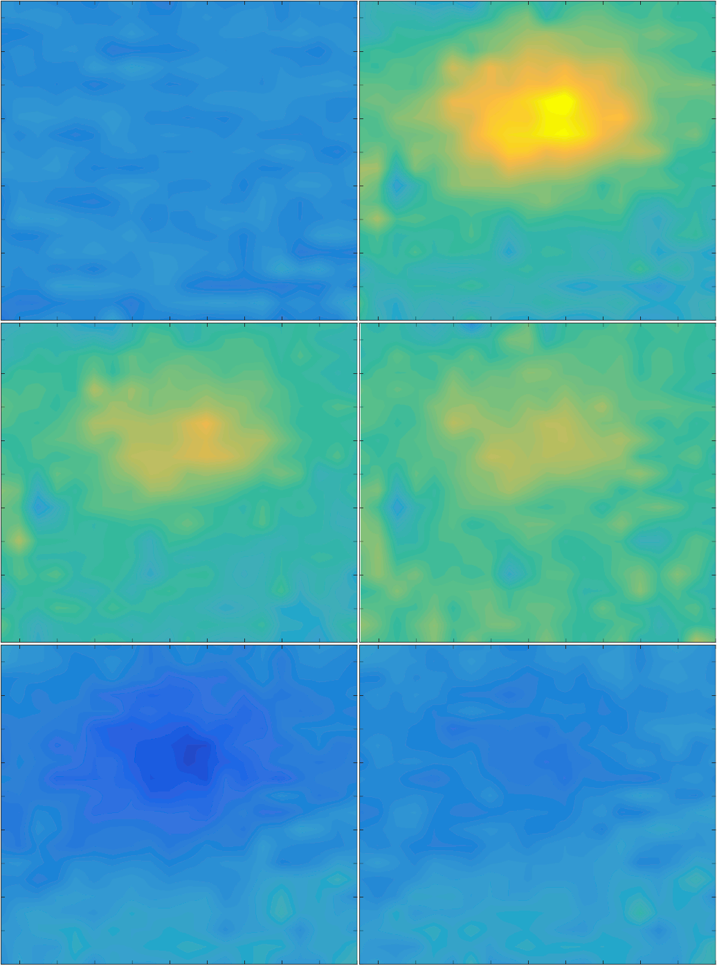
This animation shows the appearance and dissipation of an electric field recorded using the CAGE system. The strength of the field is color-coded, with yellow showing the strongest peak and dark blue showing the weakest measure. (Credit: Halleh Balch and Jason Horng/Berkeley Lab and UC Berkeley)
Other techniques have been developed to measure electrical signals from small arrays of cells, though these methods can be difficult to scale up to larger arrays and in some cases cannot trace individual electrical impulses to a specific cell.
Also, Cui said, “This new method does not perturb cells in any way, which is fundamentally different from existing methods that use either genetic or chemical modifications of the cell membrane.”
The new platform should more easily permit single-cell measurements of electrical impulses traveling across networks containing 100 or more living cells, researchers said.
Tapping graphene’s light-absorbing properties
Graphene, which is composed of a honeycomb arrangement of carbon atoms, is the focus of intense R&D because of its incredible strength, ability to very efficiently conduct electricity, high degree of chemical stability, the speed at which electrons can move across its surface, and other exotic properties. Some of this research is focused on the use of graphene as a component in computer circuits and display screens, in drug delivery systems, and in solar cells and batteries.
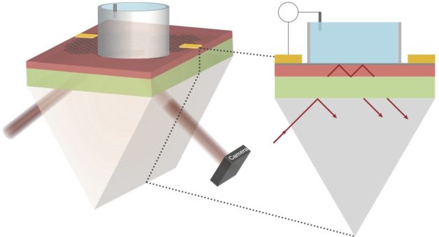
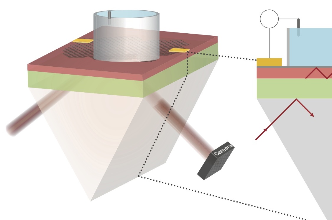
This diagram shows the setup for an imaging method that mapped electrical signals using a sheet of graphene and an infrared laser. The laser was fired through a prism (lower left) onto a sheet of graphene. An electrode was used to send tiny electrical signals into a liquid solution (in cylinder atop the graphene), and a camera (lower right) was used to capture images mapping out these electrical signals. (Credit: Halleh Balch and Jason Horng/Berkeley Lab and UC Berkeley)
In the latest study, researchers first used infrared light produced at Berkeley Lab’s Advanced Light Source to understand the effects of an electric field on graphene’s absorption of infrared light.
In the experiment, they aimed an infrared laser through a prism to a thin layer called a waveguide. The waveguide was designed to precisely match graphene’s light-absorbing properties so that all of the light was absorbed along the graphene layer in the absence of an electric field.
Researchers then fired tiny electrical pulses in a liquid solution above the graphene layer that very slightly disrupted the graphene layer’s light absorption, allowing some light to escape in a way that carried a precise signature of the electrical field. Researchers captured a sequence of images of this escaping light in thousandths-of-a-second intervals, and these images provided a direct visualization of the electrical field’s strength and location along the surface of the graphene.
Millionths-of-a-volt sensitivity
The new imaging platform—dubbed CAGE for “Critically coupled waveguide-Amplified Graphene Electric field imaging device”—proved sensitive to voltages of a few microvolts (millionths of a volt). This will make it ultrasensitive to the electric fields between cells in networks of heart cells and nerve cells, which can range from tens of microvolts to a few millivolts (thousandths of a volt).
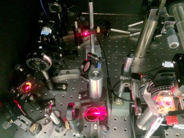
Another view of the CAGE system, with the graphene sample at lower right. (Credit: Halleh Balch and Jason Horng/Berkeley Lab, UC Berkeley)
Researchers found that they could pinpoint an electric field’s location along the graphene sheet’s surface down to tens of microns (millionths of a meter), and capture its fading strength in a sequence of time steps separated by as few as five milliseconds, or thousandths of a second.
In one sequence, researchers detailed the position and dissipation, or fade, of a local electric field generated by a 10-thousandths-of-a-volt pulse over a period of about 240 milliseconds, with sensitivity down to about 100 millionths-of-a-volt.
Next up: living heart cells
Balch said that there are already plans to test the platforms with living cells. “We are working with collaborators to test this with real heart cells,” she said. “There are several potential applications for this research in heart health and drug screening.”
There is also potential to use other atomically thin materials besides graphene in the imaging setup, she said.
“The kind of elegance behind this system comes from its generality,” Balch said. “It can be sensitive to anything that carries charge.”
The research team included participants from Berkeley Lab, UC Berkeley, and Stanford University. The work was supported by the U.S. Department of Energy Office of Science, the National Science Foundation, the David and Lucile Packard Foundation, and the Stanford University Bio-X Graduate Fellowship Program.
The Advanced Light Source is a DOE Office of Science User Facility.
###
Lawrence Berkeley National Laboratory addresses the world’s most urgent scientific challenges by advancing sustainable energy, protecting human health, creating new materials, and revealing the origin and fate of the universe. Founded in 1931, Berkeley Lab’s scientific expertise has been recognized with 13 Nobel Prizes. The University of California manages Berkeley Lab for the U.S. Department of Energy’s Office of Science. For more, visit www.lbl.gov.
DOE’s Office of Science is the single largest supporter of basic research in the physical sciences in the United States, and is working to address some of the most pressing challenges of our time. For more information, please visit science.energy.gov.
