
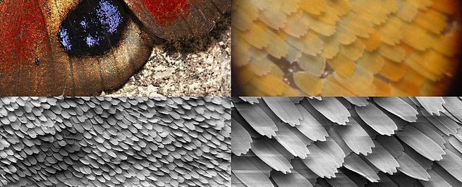
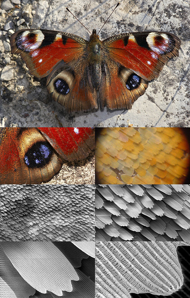
A collage of images showing butterfly wings at different magnifications. (Credit: Wikimedia Commons)
A butterfly’s wings and a peacock’s feathers use nanoscale architecture to bend light and produce brilliant colors without pigments or dyes, and scientists have been trying to emulate nature’s design.
Now, scientists from mixed reality technology company Magic Leap Inc., working with researchers at the Department of Energy’s Lawrence Berkeley National Laboratory (Berkeley Lab), have developed new, versatile ways to control and enhance the light-bending properties of synthetic optical nanostructures. Magic Leap’s technology creates visualizations that allow virtual imagery to coexist and interact with a viewer’s actual surroundings in real time.
The researchers’ achievement, reported in Scientific Reports, enables the manipulation of light over wide angles, and across the visible light spectrum, in a very efficient way. At the core of their work is a method to create two types of silicon-based, ultrathin optical components.
“We are now able to create silicon surfaces that can take in light from a large number of input angles and wavelengths with minimal loss of diffraction efficiency,” said Stefano Cabrini, director of the Nanofabrication Facility at Berkeley Lab’s Molecular Foundry, which specializes in tools and techniques for nanoscale R&D.
“The input flexibility and the degree of control these nanostructures have over the output beam has never been seen before,” Cabrini said.
Many existing optical devices are also designed to control and manipulate light for sensing, imaging, and communications, for example, but their components can be bulky and expensive, such as those used in some medical imaging machines and DSLR cameras.
Shrinking these implements down to the nanoscale could usher in a new generation of affordable devices with advanced functionality for telecommunications, medicine, and consumer products. The list of potential applications includes “smart” surfaces that can repel water, ultrafast data processing, holograms, and even “invisibility” cloaks that can conceal objects by manipulating light.
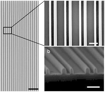
Scanning electron microscope images of the transmission mode metasurface developed at the Molecular Foundry. The scale bar for the image on the left is 2 microns and is 200 nanometers for the images on the right. (Credit: Berkeley Lab)
The new technology relies on “optical metasurfaces,” which are two-dimensional structures engineered to interact with light waves in ways that natural materials cannot. The materials can have layers that are a few billionths of a meter (nanometers) thick, and contain nanoscale optical antennas that can control the reflection or transmission of light. Their ultrathin nature makes them easy to integrate into a variety of systems.
Antireflective coatings, such as the ones used on eyeglass lenses to reduce glare, provide a simple example of optical metasurfaces. Many of these lens coatings are made of ultrathin (measured in hundreds of nanometers) transparent structures whose arrangement controls the reflection of light entering the lens.
The research team from Magic Leap created the new metasurfaces by partnering with nanofabrication experts at the Molecular Foundry. They carved a pattern of silicon nanobeams using a focused beam of electrons and then transferred the design onto an ultrathin layer of silicon, only about 20 to 120 nanometers in thickness. These nanobeams were arranged to control either the transmission or reflection of light.
These metasurfaces are a miniaturized example of diffraction gratings, which have grooved surfaces that can split and bend light, and function similarly to how a prism splits a beam of light into a rainbow. The grooves can be arranged to concentrate the diffracted light into a particular order for a given wavelength, creating specific patterns.
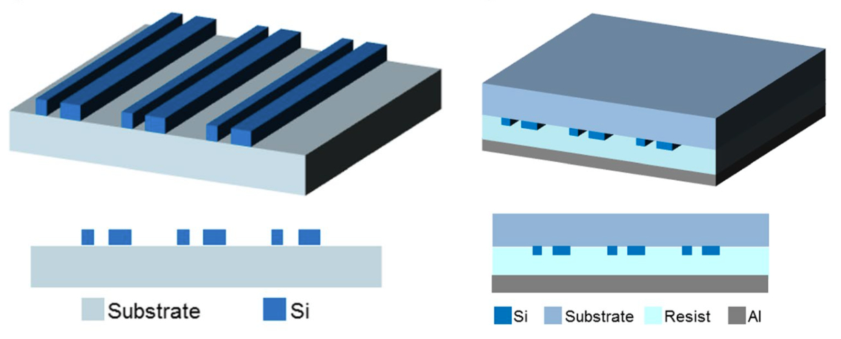
Schematics of the metasurfaces developed at the Molecular Foundry. The image on the left shows repeating pairs of silicon nanobeams, with one beam measuring 30 nanometers and the other in the pair measuring 55 nanometers across. The image at the right shows another metasurface PMMA (acrylic) material spacer layer between pairs of nanobeams and a metal layer. (Credit: Berkeley Lab)
Previous designs of metasurfaces that can control ultracompact beams of light have been functional, but limited. These structures have tended to only bend light to narrow angles because increasing the angle makes the devices inefficient.
Older designs were also constrained by both the light’s input angle and wavelength. Incoming light had to enter the surface at a 90-degree angle to avoid a drop in efficiency and was limited to wavelengths in the infrared spectrum to avoid problems with light absorption, both of which can make devices unreliable or defective.
The nanobeams that make up each of the new designs were carefully engineered to steer the light as it passes through or reflects off the surface. The size of the nanobeams and spacing between them controls the properties of the exiting light.
By making the metasurfaces out of silicon, the researchers were able to take advantage of fabrication technology that is widely available for this material, which allows their work to be more easily scaled up to mass production.
The Molecular Foundry is a DOE Office of Science User Facility that offers expert assistance and state-of-the-art equipment in nanoscale science to visiting scientists from all over the world. Work at the Molecular Foundry was supported by the Department of Energy’s Office of Science. The research team included scientists from Magic Leap, Berkeley Lab’s Molecular Foundry, and Stanford University’s Geballe Laboratory for Advanced Materials.
–By Lauren Chong