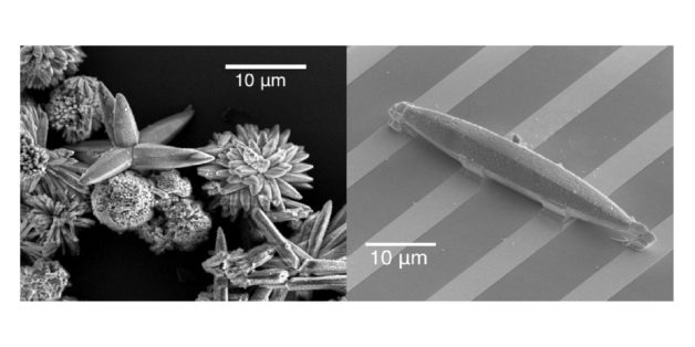
At left, a scanning electron microscopy (SEM) image of an iron BDP MOF crystal; at right, an iron BDP MOF single-crystal device bonded to a platinum microelectrode array. (Credit: Berkeley Lab)
MOFs – or metal-organic frameworks – are highly customizable porous network solids featuring cages that can come in many sizes and can attract and hold a variety of chemical components, such as carbon dioxide, methane, and hydrogen gases. And it’s this versatile specificity that gives MOFs so much potential for applications in next-generation batteries and in carbon capture, among a growing list. Despite their many positive traits, their open, porous structure – which holds on to electrons – isn’t ideal for applications that require electrons to freely flow with ions (charged particles) through a device to create an electric current.
Now, a team led by researchers at the U.S. Department of Energy’s Lawrence Berkeley National Laboratory (Berkeley Lab) and UC Berkeley has developed a technique for making an electrically conductive MOF that could also be used to improve the conductivity of other MOFs. The work was reported in Nature Materials.

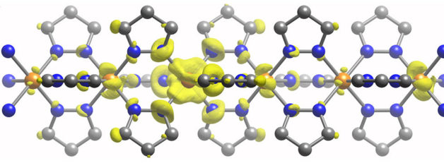
3D structure of the iron–pyrazolate chain. The iron chain acts like a wire capable of conducting electricity in an iron benzenedipyrazolate MOF crystal. (Credit: Berkeley Lab)
To work around MOFs’ inherently low electrical conductivity, the researchers added a potassium chemical mix to an iron benzenedipyrazolate (BDP) MOF. The extra electrons produced during this reaction can then enter the MOF’s iron center and conduct electricity by hopping along the length of one crystal axis of the rod-shaped crystals. The iron center acts like a wire capable of conducting electricity.
Most MOFs degrade when exposed to potassium, but the iron BDP MOF features robust triangular channels that held up during a series of tests where each reaction boosted the material’s electron count until maximum conductivity for that material was reached, resulting in a MOF that conducts electricity up to 10,000 times better than before it underwent the potassium reactions. “It’s amazing that this architecture, once incorporated into a micron-size transistor-like device, allowed us to measure the electron count as it increased with each successive potassium reaction,” said Jeffrey Long, senior faculty scientist in the Materials Sciences Division at Berkeley Lab and professor of chemistry and chemical and biomolecular engineering at UC Berkeley who served as the study’s lead author.
Another challenge in this study was growing the MOFs so that their atoms are first perfectly aligned – electrons need to travel in a straight path to generate electricity – and then wiring up these micron-size devices to measure their conductivity. “This was incredibly difficult to do,” said Long. “We weren’t able to grow very large crystals of this MOF, and the size and shape in which the crystals grow made it difficult to wire them up into a device. But we found a way around that.”
Working with the lab of Peidong Yang, a senior faculty scientist in the Materials Sciences Division at Berkeley Lab and professor of chemistry and materials science and engineering at UC Berkeley, the researchers placed platinum contacts on each side of the MOF crystal, which are just 10 microns long – the length of two red blood cells lined up side by side. The newly created MOF is a continuation of work first reported by Long’s lab in 2009.
“This MOF not only has really high electrical conductivity, but its iron chain in the center can be translated to other MOFs rather easily without losing much conductivity,” said Michael Aubrey, a former graduate student researcher in the Long group at UC Berkeley who is now a postdoctoral researcher at Stanford University.
Simulations of the MOFs’ electronic structure were led by Jeff Neaton, director of Berkeley Lab’s Molecular Foundry, a DOE Office of Science user facility specializing in nanoscience research. Diffraction work was performed at the Advanced Photon Source at Argonne National Laboratory.
This early demonstration of a highly conductive 3D MOF could bode well for its future use as an all-purpose material for batteries, supercapacitators, and fuel cells. It could also be incorporated into existing composite materials to transform them into porous conductors. And because the potassium-reduced MOF’s organic components are switchable without compromising stability or electron mobility, it could also be used to make different compounds for catalysts and electrolytes.
And the future for MOFs may be even brighter as the researchers look ahead to “boost the conductivities even further,” Long said. “If we can have this level of conductivity in a material where the electrons are moving in one dimension, we would like to one day create MOFs that have electrons mobile in two or three dimensions,” which would expand their potential for electronics and battery applications.
The Molecular Foundry and Advanced Photon Source are DOE Office of Science User Facilities.
The work was supported by the DOE Office of Science. Additional funding was provided by the National Science Foundation and the Korea Research Institute of Chemical Technology.
###
Lawrence Berkeley National Laboratory addresses the world’s most urgent scientific challenges by advancing sustainable energy, protecting human health, creating new materials, and revealing the origin and fate of the universe. Founded in 1931, Berkeley Lab’s scientific expertise has been recognized with 13 Nobel Prizes. The University of California manages Berkeley Lab for the U.S. Department of Energy’s Office of Science. For more, visit http://www.lbl.gov.
DOE’s Office of Science is the single largest supporter of basic research in the physical sciences in the United States, and is working to address some of the most pressing challenges of our time. For more information, please visit the Office of Science website at science.energy.gov.
