

Three technologies from the U.S. Department of Energy’s (DOE) Lawrence Berkeley National Laboratory (Berkeley Lab) have won a 2021 R&D 100 award, representing innovations for memory and logic chips, next-generation batteries, and radiation detection and mapping.
Presented by R&D Magazine, the R&D 100 Awards, which are selected by an independent panel of judges, recognize the year’s 100 most innovative and disruptive technology products from industry, academia, and government-sponsored research. Established in 1963, the R&D 100 Awards is the only science and technology awards competition that recognizes new commercial products, technologies, and materials for their technological significance that are available for sale or license.
Go here to see all of the winners. The three awards this year brings the total of Berkeley Lab R&D 100 wins to 108, including two Editors’ Choice Awards. The winners were honored in virtual awards ceremonies from Oct. 19-21, 2021.
Following are descriptions of the winning technologies:
A new lithography photomask material for mass production of logic and memory chips
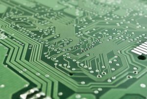
Components that go onto chips are getting smaller and smaller, but current methods for copying patterns onto wafers are limited in their precision. (Credit: Pixabay/Michael Schwarzenberger)
Manufacturers of devices like smartphones or computers are continually trying to scale down the components that go onto each system-on-a-chip (SOC) in order to add performance and power without significantly raising costs. This downscaling is achieved using photolithography, which is the approach that enables high-volume manufacturing by rapidly copying the layout of a pattern from a photomask onto a target wafer. The technique is limited by the size of the wavelengths, and so downscaling has required increasingly shorter wavelengths.
A new photolithography technology called extreme ultraviolet lithography (EUVL), which uses extremely small-wavelength light and is capable of patterning very small features, has recently been deployed at the largest chip makers, but one challenge of the new technology is the thickness of the mask pattern that is required to ensure typical absorber materials are dark enough to sufficiently block the light. Berkeley Lab scientists have created a new, darker absorber material, chromium-antimony, that results in high-quality nanometer films and can be patterned with a high degree of control and resolution, down to 5 nanometers. The invention promises high resolution, single exposure, and cost-effective patterning for the fabrication of logic and memory chips.
Investigators: Daniel Staaks (PI), Stefano Cabrini (Molecular Foundry), Patrick Naulleau, Farhad Salmassi, Eric Gullikson (Center for X-ray Optics, Materials Sciences Division)
A novel cathode material for next-generation lithium-ion batteries
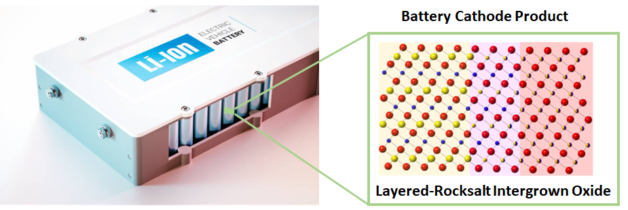
The cathode in the Berkeley Lab invention uses a novel layered-rocksalt intergrown oxide material. (Credit: Berkeley Lab/Wei Tong)
The $30 billion-plus global lithium-ion battery market is expected to double in the next five years, with high performance, safe batteries critical to many industries. However, at high voltage, cathode materials currently used for Li-ion batteries degrade and show significant declining performance over time, limiting their usefulness in many key applications.
Improved cathode materials could help batteries operate reliably at high capacity and high voltage over repeated cycles without sacrificing performance, safety, or cost. Berkeley Lab scientists have developed a unique cathode material that uses a layered- rocksalt intergrown structure, combining the high capacity of lithium-rich metal oxides, fast kinetics of a cation-ordered layered structure, along with structural stability of a cation-disordered rocksalt structure. Such a material has been shown to offer high capacity, fast charging time and energy transfer, and superior cycling and thermal stability. In addition, the cost for raw materials to produce layered-rocksalt intergrown electrodes is estimated to be significantly less than that of lithium-rich layered oxides when expensive cobalt is completely replaced by cost-effective iron. This innovation exemplifies a new battery electrode design concept and opens up a new class of high-performance intergrown cathode materials.
Investigators: Wei Tong (PI), Ning Li, Meiling Sun, Jing Xu (Energy Technologies Area) and Wanli Yang (Energy Sciences Area)
A 3D, real-time radiation detection and mapping platform
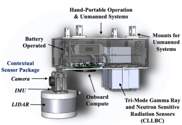
The lightweight NG-LAMP device includes LiDAR and visual sensors, radiation sensors, and a computing component. (Credit: Berkeley Lab/Josh Cates)
Detection and mapping of radiation sources is critical for international security, nuclear reactor safety, and decontamination efforts. Berkeley Lab scientists developed the Neutron and Gamma Ray Source Localization and Mapping Platform (NG-LAMP), the first real-time platform for mapping gamma ray and neutron sources in three dimensions. 3D maps can pinpoint contamination or hotspots to specific areas or objects better than 2D approaches used by the current portable radiation imaging systems in the market, enabling more efficient planning and response.
The NG-LAMP platform employs Berkeley Lab-developed Scene Data Fusion, which provides 3D, high resolution nuclear radiation maps with data from sensors on the device (including LiDAR and visual sensors) and radiation data. A Berkeley Lab-developed software suite, dubbed the Localization and Mapping Platform, combines the data collected by the device, and, in real time, the onboard computing unit uses the data to produce 3D reconstructions of the radioactivity (without transmitting sensor data and performing computation on an external platform). The 3D maps are then transmitted to the user over WiFi.
The lightweight device is suitable for portable operations and for operations on unmanned aerial and ground vehicles. Such a capability can support the U.S. military, international inspectors, and law enforcement in locating radiation sources, as well as support nuclear reactor emergency response and decontamination efforts.
Investigators: Joshua Cates (PI), Ryan Pavlovsky, Victor Negut, Brian Quiter, Tenzing Joshi, Alex Moran (Physical Sciences Area)
###
Founded in 1931 on the belief that the biggest scientific challenges are best addressed by teams, Lawrence Berkeley National Laboratory and its scientists have been recognized with 14 Nobel Prizes. Today, Berkeley Lab researchers develop sustainable energy and environmental solutions, create useful new materials, advance the frontiers of computing, and probe the mysteries of life, matter, and the universe. Scientists from around the world rely on the Lab’s facilities for their own discovery science. Berkeley Lab is a multiprogram national laboratory, managed by the University of California for the U.S. Department of Energy’s Office of Science.
DOE’s Office of Science is the single largest supporter of basic research in the physical sciences in the United States, and is working to address some of the most pressing challenges of our time. For more information, please visit energy.gov/science.