While a movie about giant robots that undergo structural transformations is breaking box office records this summer, a scientific study about structural transformations within single nanocrystals is breaking new ground for the design of novel materials that will serve next-generation energy storage batteries and solar energy harvesting devices. Researchers at the U.S. Department of Energy (DOE)’s Lawrence Berkeley National Laboratory (Berkeley Lab) have reported the first direct observation of structural transformations within a single nanocrystal of copper sulfide, a semiconductor expected to play an important role in future energy technologies.

Fast Fourier transform pattern (left) and high resolution TEM images of the low-chalcocite (green) and high-chalcocite (red) domains in a copper sulfide nanorod
Using TEAM 0.5, one of the world’s most powerful transmission electron microscopes, a research group led by Berkeley Lab director Paul Alivisatos, observed structural fluctuations in a copper sulfide nanocrystal as it transitioned between the low- and high-chalcocite solid-state phases. These fluctuations are highly relevant to understanding such phenomena as how ion transport occurs within electrodes during the charging and discharging of batteries, or how the structures of a solid material might change at the interface between an electrode and an electrolyte.
“TEAM 0.5, with its advanced electron optics and recording systems, enables rapid sample imaging with single atom sensitivity across the periodic table and greater collection efficiency. This provides extraordinary opportunities to study structural transformation dynamics in situ with atomic resolution,” Alivisatos says.
“In this study,” he adds, “we observed structural transformation dynamics in a copper sulfide nanorod from a low- to a high-chalcocite structure with unprecedented detail, and found these dynamics to be strongly influenced by defects in the nanorod crystal. Our findings suggest strategies for suppressing or assisting such transformations that should aid in the future design of materials with new and controlled phases.”

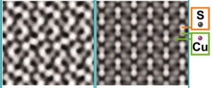
TEAM 0.5 micrographs showing the low-chalcocite (left) and high-chalcocite atomic structures of a copper sulfide nanorod.
The popular concept of phase transitions is that of a material, in response to temperature changes, undergoing a transformation from a solid to a liquid or gas, i.e., ice to water to steam. But some solid materials, especially at the nanoscale, when subjected to temperature changes can transition between two more different phases in their crystal structure. Copper sulfide, for example, can be transformed from a complex hexagonal structure known as the low-chalcocite phase, to a more simple hexagonal structure known as the high-chalcocite phase. Because such “first-order structural transformations” can alter the properties of a nanocrystal, they are of great interest to a broad range of scientific fields and hold important implications for numerous technologies.
“In nanoscale systems, the energetic barrier to a structural transformation scales with crystal size,” says Alivisatos. “When the size of a nanocrystal is in a regime where thermal energy is comparable to the energy barrier for phase transformation, fluctuations between two stable structures occur at the transition point, and are relevant to many molecular and solid-state phenomena near equilibrium.”
Alivisatos, the Larry and Diane Bock Professor of Nanotechnology at the University of California (UC) Berkeley, is a corresponding author of a paper in the journal Science titled “Observation of Transient Structural-Transformation Dynamics in a Cu2S Nanorod.” Co-authoring this paper were Haimei Zheng, Jessy Rivest, Timothy Miller, Bryce Sadtler, Aaron Lindenberg, Michael Toney, Lin-Wang Wang and Christian Kisielowski.

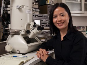
Haimei Zheng, is a staff Scientist in Berkeley Lab’s Materials Sciences Division and a DOE Early Career Research Program Awardee (2011). She and a team that included Paul Alivisatos reported the first direct observation of structural transformations within a single nanocrystal of copper sulfide. (Photo by Roy Kaltschmidt, Berkeley Lab)
“During the phase transitions of copper sulfide between low-chalcocite and high-chalcocite structure, the sulfur ions remain in a rigid lattice frame while the copper ions move within the sulfur ion lattice,” says Haimei Zheng, lead and co-corresponding author of the Science paper.
“We observed where the phase nucleates at the surface of the nanorod and within the core and how the phase transformation propagates,” Zheng says. “We also observed the effects of defects. For example, we observed that a stacking fault creates a barrier for the movement of copper ions and thereby blocks the phase propagation. Such observations provide us with important new insights on the atomic pathways of first order structural transformations.”
According to phase transition theory, a solid crystal will fluctuate between two equilibrium structures near the phase transition point before reaching a stable configuration, and that this region of transition broadens in small crystals. To test this theory, Zheng, Alivisatos and their co-authors zapped copper sulphide nanorods with an electron beam from the TEAM 0.5 microscope then watched for and saw the predicted fluctuations.
“Before the TEAM microscopes, such details of the fluctuations between two solid-state phases in a nanocrystal could not have been observed,” says Zheng. “Our results should be of interest to theorists attempting to simulate structural transformations in solids as neither a study on bulk materials nor on the ensemble of nanomaterials has the capability of revealing such specific features of the phase transition pathways.”
TEAM stands for Transmission Electron Aberration-corrected Microscope. TEAM 0.5 and its sister instrument TEAM 1.0 are capable of producing images with half‑angstrom resolution – less than the diameter of a single hydrogen atom. Both microscopes are housed at Berkley Lab in DOE’s National Center for Electron Microscopy (NCEM).
The next step for her, Zheng says, will be to address questions concerning the transport of ions with battery material changes at the electrode/electrolyte interface, and structural changes of nanoparticle catalysts.
“Such studies share the same aim of developing microscopic understanding of the structural transformations of materials, especially those that are important for energy applications,” Zheng says. “In situ transmission electron microscopy, especially our recent technical advances in dynamic imaging through liquids or gases, as well as at the applied electric biasing, provides a powerful tool for such studies.”
This research was supported by the DOE Office of Science.
Lawrence Berkeley National Laboratory addresses the world’s most urgent scientific challenges by advancing sustainable energy, protecting human health, creating new materials, and revealing the origin and fate of the universe. Founded in 1931, Berkeley Lab’s scientific expertise has been recognized with 12 Nobel prizes. The University of California manages Berkeley Lab for the U.S. Department of Energy’s Office of Science. For more, visit www.lbl.gov.
Additional information:
For more information about the research of Paul Alivisatos, visit the Website at http://www.cchem.berkeley.edu/pagrp/
For more information on the National Center for Electron Microscopy visit the Website at http://ncem.lbl.gov/
For more information about the research of Haimei Zheng, visit her Website at http://ncem.lbl.gov/Haimei/