If nanoscience were television, we’d be in the 1950s. Although scientists can make and manipulate nanoscale objects with increasingly awesome control, they are limited to black-and-white imagery for examining those objects. Information about nanoscale chemistry and interactions with light—the atomic-microscopy equivalent to color—is tantalizingly out of reach to all but the most persistent researchers.
But that may all change with the introduction of a new microscopy tool from researchers at the Department of Energy (DOE)’s Lawrence Berkeley National Laboratory (Berkeley Lab) that delivers exquisite chemical details with a resolution once thought impossible. The team developed their tool to investigate solar-to-electric energy conversion at its most fundamental level, but their invention promises to reveal new worlds of data to researchers in all walks of nanoscience.

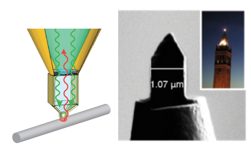
A new microscopy tool promises to revolutionize nanoscale imaging. Left, a design schematic of the so-called “campanile” microscopy tip. Right, an electron micrograph of the tip and, inset, the UC Berkeley campanile bell-tower for which it is named.
“We’ve found a way to combine the advantages of scan/probe microscopy with the advantages of optical spectroscopy,” says Alex Weber-Bargioni, a scientist at the Molecular Foundry, a DOE nanoscience center at Berkeley Lab. “Now we have a means to actually look at chemical and optical processes on the nanoscale where they are happening.”
Weber-Bargioni is one of the corresponding authors of a paper reporting this research, published in Science. The paper is titled, “Mapping local charge recombination heterogeneity by multidimensional nanospectroscopic imaging.” Co-authoring the paper are Wei Bao, Mauro Meli, Frank Ogletree, Shaul Aloni, Jeffrey Bokor, Stephano Cabrini, Miquel Salmeron, Eli Yablonovitch, and James Schuck of Berkeley Lab; Marco Staffaroni of the University of California, Berkeley; Hyuck Choo of Caltech; and their colleagues in Italy, Niccolo Caselli, Francesco Riboli, Diederik Wiersma, and Francesca Intoni.
“If you want to characterize materials, particularly nanomaterials, the way it’s traditionally been done is with electron microscopies and scan/probe microscopies because those give you really high, sub-atomic spatial resolution,” says co-author James Schuck, a nano-optics researcher at the Molecular Foundry. “Unfortunately, what they don’t give you is chemical, molecular-level information.”
For chemical information, researchers typically turn to optical or vibrational spectroscopy. The way a material interacts with light is dictated to large part by its chemical composition, but for nanoscience the problem with doing optical spectroscopy at relevant scales is the diffraction limit, which says you can’t focus light down to a spot smaller than approximately half its wavelength, due to the wave-nature of light.
To get around the diffraction limit, scientists employ “near-field” light. Unlike the light we can see, near-field light decays exponentially away from an object, making it hard to measure, but it contains very high resolution—much higher than normal, far-field light.
Says Schuck, “The real challenge to near-field optics, and one of the big achievements in this paper, is to create a device that acts as a transducer of far-field light to near-field light. We can squeeze it down and get very enhanced local fields that can interact with matter. We can then collect any photons that are scattered or emitted due to this interaction, collect in the near field with all this spatial frequency information and turn it back into propagating, far-field light.”

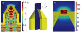
Electromagnetic fields are enhanced in the gap as the campanile squeezes light beyond the diffraction limit, as shown in these simulations.
The trick for that conversion is to use surface plasmons: collective oscillations of electrons that can interact with photons. Plasmons on two surfaces separated by a small gap can collect and amplify the optical field in the gap, making a stronger signal for scientists to measure.
Researchers have exploited these effects to make near-field probes with a variety of geometries, but the experiments typically require painstaking optical alignment, suffer from background noise, only work for narrow frequency ranges of light and are limited to very thin samples.

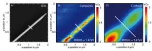
Using the campanile tip, Berkeley Lab researchers take “color” images with nanoscale resolution. A photovoltaic indium-phosphide nanowire is easy to see in a black-and-white electron micrograph (left) but chemical information has low resolution in a normal confocal micrograph (right). The campanile tip reveals both shape and chemistry of a nanowire (center).
In this latest work, however, the Berkeley Lab researchers transcended these limitations with a cleverly designed near-field probe. Fabricated on the end of an optical fiber, the probe has a tapered, four-sided tip. The researchers named their new tool after the campanile church tower it resembles, inspired by the landmark clock tower on the UC Berkeley campus. Two of the campanile’s sides are coated with gold and the two gold layers are separated by just a few nanometers at the tip. The three-dimensional taper enables the device to channel light of all wavelengths down into an enhanced field at the tip. The size of the gap determines the resolution.
In a regular atomic force microscope (AFM), a sharp metal tip is essentially dragged across a sample to generate a topological map with sub-nanoscale resolution. The results can be exquisite but only contain spatial information and nothing about the composition or chemistry of the sample.
Replacing the usual AFM tip with a campanile tip is like going from black-and-white to full color. You can still get the spatial map but now there’s a wealth of optical data for every pixel on that map. From optical spectra, scientists can identify atom and molecule species, and extract details about electronic structure.
“That’s the beauty of these tips,” says Schuck. “You can just put them on the end of an optical fiber and then it’s just like using a regular AFM. You don’t have to be a super near-field jock anymore to get this type of data.”
The team developed their new tool to study indium-phosphide nanowires. These nanowires, with the nearly ideal band gap of 1.4 electron-volts, are well-suited to converting solar energy to electricity. The researchers found that the nanowires were not the homogeneous objects previously thought, but instead had varying optoelectronic properties along their length, which could radically alter how sunlight is converted to electricity. They also found that photoluminescence, an indication of the relationship between light and electricity, was seven-times stronger in some parts of a nanowire than others. This is the first time anyone has measured these events on such a small scale.
Weber-Bargioni says: “Details like this about indium-phosphide nanowires are important because if you want to use these suckers for photocatalysis or a photovoltaic material then the length scale at which we’re measuring is where everything happens. This information is really important to understand how, for example, the fabrication and surface treatment of nanowires influences these charge recombination velocities. These determine how efficiently a solar device can convert photons into usable electrons.”
Adds Schuck: “We realized that this is really the optimal way to do any kind of optical experiment one might want to do at the nano scale. So we use it for imaging and spectroscopy but we anticipate many other uses also.”
Experiments were carried out in collaboration with the groups of Diederik Wiersma and Francesca Intonti from the European Laboratory for Non-linear Spectroscopy, Italy.
This research was supported by the DOE Office of Science.
# # #
Lawrence Berkeley National Laboratory addresses the world’s most urgent scientific challenges by advancing sustainable energy, protecting human health, creating new materials, and revealing the origin and fate of the universe. Founded in 1931, Berkeley Lab’s scientific expertise has been recognized with 13 Nobel prizes. The University of California manages Berkeley Lab for the U.S. Department of Energy’s Office of Science. For more, visit www.lbl.gov.
The Molecular Foundry is one of five DOE Nanoscale Science Research Centers (NSRCs), national user facilities for interdisciplinary research at the nanoscale, supported by the DOE Office of Science. Together the NSRCs comprise a suite of complementary facilities that provide researchers with state-of-the-art capabilities to fabricate, process, characterize, and model nanoscale materials, and constitute the largest infrastructure investment of the National Nanotechnology Initiative. The NSRCs are located at DOE’s Argonne, Brookhaven, Lawrence Berkeley, Oak Ridge and Sandia and Los Alamos national laboratories. For more information about the DOE NSRCs, please visit http://science.energy.gov/bes/suf/user-facilities/nanoscale-science-research-centers/.
DOE’s Office of Science is the single largest supporter of basic research in the physical sciences in the United States, and is working to address some of the most pressing challenges of our time. For more information, please visit the Office of Science website at science.energy.gov/.
Additional Information:
For more information about the Molecular Foundry go here
For more information about the research of Jim Schuck go here
