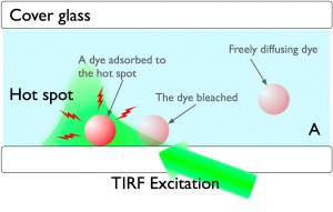
Multiple nano-sized electromagnetic hotspots on aluminum are identified in the movie on left by the “blinking” pattern, with each blink corresponding to a single molecule adsorption event. Spot marked by the red arrow is singled out to illustrate the image reconstruction process in the right panel. Every single molecule adsorption event is used as a 3D coordinate to assemble the profile of the field distribution on the right. (Movie courtesy of Zhang group.)
The secrets behind the mysterious nano-sized electromagnetic “hotspots” that appear on metal surfaces under a light are finally being revealed with the help of a BEAST. Researchers at the U.S. Department of Energy (DOE)’s Lawrence Berkeley National Laboratory (Berkeley Lab) have developed a single molecule imaging technology, dubbed the Brownian Emitter Adsorption Super-resolution Technique (BEAST), that has made it possible for the first time to directly measure the electromagnetic field inside a hotspot. The results hold promise for a number of technologies, including solar energy and chemical sensing.
“With our BEAST method, we were able to map the electromagnetic field profile within a single hotspot as small as 15 nanometers with an accuracy down to 1.2 nanometers, in just a few minutes,” says Xiang Zhang, a principal investigator with Berkeley Lab’s Materials Sciences Division and the Ernest S. Kuh Endowed Chaired Professor at the University of California (UC), Berkeley. “We discovered that the field is highly localized and, unlike a typical electromagnetic field, does not propagate through space. The field also has an exponential shape that rises steeply to a peak and then decays very fast.”
Zhang, who directs the Center for Scalable and Integrated NanoManufacturing (SINAM), a National Science Foundation Nano-scale Science and Engineering Center at UC Berkeley, is the corresponding author of a paper on this research that appears in the journal Nature under the title “Mapping the Distribution of Electromagnetic Field Inside a 15nm Sized Hotspot by Single Molecule Imaging.” Co-authoring the paper with Zhang were Hu Cang, Anna Labno, Changgui Lu, Xiaobo Yin, Ming Liu and Christopher Gladden.
Under optical illumination, rough metallic surfaces will become dotted with microscopic hotspots, where the light is strongly confined in areas measuring tens of nanometers in diameter, and the Raman (inelastic) scattering of the light is enhanced by up to 14 orders of magnitude. First observed more than 30 years ago, such hotspots have been linked to the impact of surface roughness on plasmons (electronic surface waves) and other localized electromagnetic modes.
However, during the past three decades, little has been learned about the origins of these hotspots.

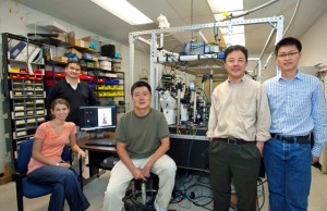
From left Anna Labno, Xiaobo Yin, Hu Cang, Xiang Zhang and Changgui Lu have developed a single molecule imaging technology, dubbed BEAST, that makes it possible to directly measure the field itensity inside an electromagnetic hotspot. (Photo by Roy Kaltschmidt, Berkeley Lab Public Affairs)
“Amazingly, despite thousands of papers on this problem and various theories, we are the first to experimentally determine the nature of the electromagnetic field inside of such a nano-sized hotspots,” says Hu Cang, lead author on the Nature paper and a member of Zhang’s research group. “The 15 nanometer hotspot we measured is about the size of a protein molecule. We believe there are hotspots that may even be smaller than a molecule.”
Because the size of these metallic hotspots is far smaller than the wavelength of incident light, a new technique was needed to map the electromagnetic field within a hotspot. The Berkeley researchers developed the BEAST method to capitalize on the fact that individual fluorescent dye molecules can be localized with single nanometer accuracy. The fluorescence intensity of individual molecules adsorbed on the surface provides a direct measure of the electromagnetic field inside a single hotspot. BEAST utilizes the Brownian motion of single dye molecules in a solution to make the dyes scan the inside of single hotspot stochastically, one molecule at a time.
“The exponential shape we found for the electromagnetic field within a hotspot is direct evidence for the existence of a localized electromagnetic field, as opposed to the more common form of Gaussian distribution,” Cang says. “There are several competing mechanisms proposed for hotspots and we are now working to further examine these fundamental mechanisms.”
 BEAST starts with the submerging of a sample in a solution of freely diffusing fluorescent dye. Since the diffusion of the dye is much faster than the image acquisition time (0.1 milliseconds vs. 50-to-100 milliseconds), the fluorescence produces a homogeneous background. When a dye molecule is adsorbed onto the surface of a hotspot, it appears as a bright spot in images, with the intensity of the spot reporting the local field strength.
“By using a maximum likelihood single molecule localization method, the molecule can be localized with single nanometer accuracy,” Zhang says. “After the dye molecule is bleached (typically within hundreds of milliseconds), the fluorescence disappears and the hotspot is ready for the next adsorption event.”
Choosing the right concentration of the dye molecules enables the adsorption rate on the surface of a hotspot to be controlled so that only one adsorbed molecule emits photons at a time. Since BEAST uses a camera to record the single molecule adsorption events, multiple hotspots within a field of view of up to one square millimeter can be imaged in parallel.
In their paper, Zhang and his colleagues see hotspots being put to use in a broad range of applications, starting with the making of highly efficient solar cells and devices that can detect weak chemical signals.
“A hotspot is like a lens that can focus light to a small spot with a focusing power well beyond any conventional optics,” Cang says. “While a conventional lens can only focus light to a spot about half the wavelength of visible light (about 200-300 nanometers), we now confirm that a hotspot can focus light to a nanometer-sized spot.”
Through this exceptional focusing power, hotspots could be used to concentrate sun light on the photocatalytic sites of solar devices, thereby helping to maximize light- harvesting and water-splitting efficiencies. For the detection of weak chemical signals, e.g., from a single molecule, a hotspot could be used to focus incident light so that it only illuminates the molecule of interest, thereby enhancing the signal and minimizing the background.
BEAST also makes it possible to study the behavior of light as it passes through a nanomaterial, a critical factor for the future development of nano-optics and metamaterial devices. Current experimental techniques suffer from limited resolution and are difficult to implement on the truly nanoscale.
“BEAST offers an unprecedented opportunity to measure how a nanomaterial alters the distribution of light, which will guide the development of advanced nano-optics devices,” says Cang. “We will also use BEAST to answer some challenging problems in surface science, such as where and what are the active sites in a catalyst, how the energy or charges transfer between molecules and a nanomaterial, and what determine surface hydrophobicity. These problems require a technique with electron-microscopy level resolution and optical spectroscopy information. BEAST is a perfect tool for these problems.”
This research was supported by DOE’s Office of Science.
Lawrence Berkeley National Laboratory is a U.S. Department of Energy (DOE) national laboratory managed by the University of California for the DOE Office of Science. Berkeley Lab provides solutions to the world’s most urgent scientific challenges including sustainable energy, climate change, human health, and a better understanding of matter and force in the universe. It is a world leader in improving our lives through team science, advanced computing, and innovative technology. Visit our Website at www.lbl.gov
Additional Information
For more information about the research of Xiang Zhang visit http://xlab.me.berkeley.edu/xlabnews.htm
For more information about the Berkeley Nano-scale Science and Engineering Center visit http://www.nanowerk.com/nanotechnology/labs/UC_Berkeley_NSF_Nanoscale_Science_and_Engineering_Center_%28SINAM%29.html