Scientific Contact: Xiang Zhang, 510-225-8559, or [email protected]
They said it could be done and now they’ve done it. What’s more, they did it with a GRIN. A team of researchers with the U.S. Department of Energy (DOE)’s Lawrence Berkeley National Laboratory (Berkeley Lab) and the University of California, Berkeley, have carried out the first experimental demonstration of GRIN – for gradient index – plasmonics, a hybrid technology that opens the door to a wide range of exotic optics, including superfast computers based on light rather than electronic signals, ultra-powerful optical microscopes able to resolve DNA molecules with visible light, and “invisibility” carpet-cloaking devices.

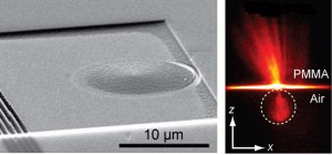
On left is a scanning electron micrograph of a plasmonic Luneburg lens on a gold film. On the right, fluorescence imaging shows intensity of the SPPs propagated by the Luneburg lens (dotted circle). X marks the launching position of the electron beam and Z is the direction in which the SPPs propogate. (Image courtesy of Zhang group)
Working with composites featuring a dielectric (non-conducting) material on a metal substrate, and “grey-scale” electron beam lithography, a standard method in the computer chip industry for patterning 3-D surface topographies, the researchers have fabricated highly efficient plasmonic versions of Luneburg and Eaton lenses. A Luneburg lens focuses light from all directions equally well, and an Eaton lens bends light 90 degrees from all incoming directions.
“This past year, we used computer simulations to demonstrate that with only moderate modifications of an isotropic dielectric material in a dielectric-metal composite, it would be possible to achieve practical transformation optics results,” says Xiang Zhang, who led this research. “Our GRIN plasmonics technique provides a practical way for routing light at very small scales and producing efficient functional plasmonic devices.”

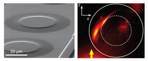
On left, a scanning electron micrograph of Eaton lenses on a gold film. On right, fluorescence imaging shows the intensity of SPPs propagating in z-direction (arrow) and bending to the right when passing through an Eaton lens. The solid line marks the outer diameter of the lens and the dashed line marks the high index region. (Image by Zhang group)
Zhang, a principal investigator with Berkeley Lab’s Materials Sciences Division and director of UC Berkeley’s Nano-scale Science and Engineering Center (SINAM), is the corresponding author of a paper in the journal Nature Nanotechnology, describing this work titled, “Plasmonic Luneburg and Eaton Lenses.” Co-authoring the paper were Thomas Zentgraf, Yongmin Liu, Maiken Mikkelsen and Jason Valentine.
GRIN plasmonics combines methodologies from transformation optics and plasmonics, two rising new fields of science that could revolutionize what we are able to do with light. In transformation optics, the physical space through which light travels is warped to control the light’s trajectory, similar to the way in which outer space is warped by a massive object under Einstein’s relativity theory. In plasmonics, light is confined in dimensions smaller than the wavelength of photons in free space, making it possible to match the different length-scales associated with photonics and electronics in a single nanoscale device.
“Applying transformation optics to plasmonics allows for precise control of strongly confined light waves in the context of two-dimensional optics,” Zhang says. “Our technique is analogous to the well-known GRIN optics technique, whereas previous plasmonic techniques were realized by discrete structuring of the metal surface in a metal-dielectric composite.”
Like all plasmonic technologies, GRIN plasmonics starts with an electronic surface wave that rolls through the conduction electrons on a metal. Just as the energy in a wave of light is carried in a quantized particle-like unit called a photon, so, too, is plasmonic energy carried in a quasi-particle called a plasmon. Plasmons will interact with photons at the interface of a metal and dielectric to form yet another quasi-particle, a surface plasmon polariton (SPP).
The Luneburg and Eaton lenses fabricated by Zhang and his co-authors interacted with SPPs rather than photons. To make these lenses, the researchers worked with a thin dielectric film (a thermplastic called PMMA) on top of a gold surface. When applying grey-scale electron beam lithography, the researchers exposed the dielectric film to an electron beam that was varied in dosage (charge per unit area) as it moved across the film’s surface. This resulted in highly controlled differences in film thickness across the length of the dielectric that altered the local propagation of SPPs. In turn, the “mode index,” which determines how fast the SPPs will propagate, is altered so that the direction of the SPPs can be influenced.

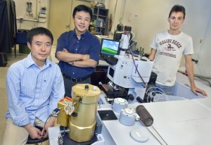
Yongmin Liu (left) Xiang Zhang and Thomas Zentgraf are three of the major authors of a Nature Nanotechnology paper describing GRIN plasmonics, a practical method for achieving exotic optics. Not shown is author Maiken Mikkelsen. (Photo by Roy Kaltschmidt, Berkeley Lab Public Affairs)
“By adiabatically tailoring the topology of the dielectric layer adjacent to the metal surface, we’re able to continuously modify the mode index of SPPs,” says Zentgraf. “As a result, we can manipulate the flow of SPPs with a greater degree of freedom in the context of two-dimensional optics.”
Says Liu, “The practicality of working only with the purely dielectric material to transform SPPs is a big selling point for GRIN plasmonics. Controlling the physical properties of metals on the nanometer length-scale, which is the penetration depth of electromagnetic waves associated with SPPs extending below the metal surfaces, is beyond the reach of existing nanofabrication techniques.”
Adds Zentgraf, “Our approach has the potential to achieve low-loss functional plasmonic elements with a standard fabrication technology that is fully compatible with active plasmonics.”
In the Nature Nanotechnology paper, the researchers say that inefficiencies in plasmonic devices due to SPPs lost through scattering could be reduced even further by incorporating various SPP gain materials, such as fluorescent dye molecules, directly into the dielectric. This, they say, would lead to an increased propagation distance that is highly desired for optical and plasmonic devices. It should also enable the realization of two-dimensional plasmonic elements beyond the Luneburg and Eaton lenses.
Says Mikkelsen, “GRIN plasmonics can be immediately applied to the design and production of various plasmonic elements, such as waveguides and beam splitters, to improve the performance of integrated plasmonics. Currently we are working on more complex, transformational plasmonic devices, such as plasmonic collimators, single plasmonic elements with multiple functions, and plasmonic lenses with enhanced performance.”
This research was supported by the U.S. Army Research Office and the National Science Foundation’s Nano-scale Science and Engineering Center.
Lawrence Berkeley National Laboratory is a U.S. Department of Energy (DOE) national laboratory managed by the University of California for the DOE Office of Science. Berkeley Lab provides solutions to the world’s most urgent scientific challenges including sustainable energy, climate change, human health, and a better understanding of matter and force in the universe. It is a world leader in improving our lives through team science, advanced computing, and innovative technology. Visit our Website at www.lbl.gov
Additional Information
For more information about the research of Xiang Zhang visit http://xlab.me.berkeley.edu/xlabnews.htm