Schematic shows how to make core/shell nanowire solar cell starting from left with a CdS nanowire (green) that is dipped in CuCl where cation exchange reaction creates a Cu2S shell coating (brown). Metal contacts are then deposited on the CdS core and Cu2S shell. (Image courtesy of Yang, et. al)
Solar or photovoltaic cells represent one of the best possible technologies for providing an absolutely clean and virtually inexhaustible source of energy to power our civilization. However, for this dream to be realized, solar cells need to be made from inexpensive elements using low-cost, less energy-intensive processing chemistry, and they need to efficiently and cost-competitively convert sunlight into electricity. A team of researchers with the U.S. Department of Energy (DOE)’s Lawrence Berkeley National Laboratory (Berkeley Lab) has now demonstrated two out of three of these requirements with a promising start on the third.
Peidong Yang, a chemist with Berkeley Lab’s Materials Sciences Division, led the development of a solution-based technique for fabricating core/shell nanowire solar cells using the semiconductors cadmium sulfide for the core and copper sulfide for the shell. These inexpensive and easy-to-make nanowire solar cells boasted open-circuit voltage and fill factor values superior to conventional planar solar cells. Together, the open-circuit voltage and fill factor determine the maximum energy that a solar cell can produce. In addition, the new nanowires also demonstrated an energy conversion efficiency of 5.4-percent, which is comparable to planar solar cells.
“This is the first time a solution based cation-exchange chemistry technique has been used for the production of high quality single-crystalline cadmium sulfide/copper sulfide core/shell nanowires,” Yang says. “Our achievement, together with the increased light absorption we have previously demonstrated in nanowire arrays through light trapping, indicates that core/shell nanowires are truly promising for future solar cell technology.”

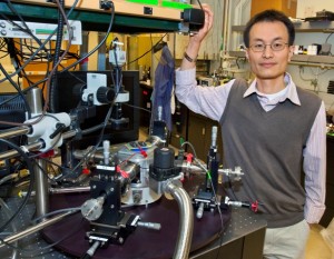
Berkeley Lab chemist Peidong Yang is a leading authority on semiconductor nanowires. (Photo by Roy Kaltschmidt, Berkely Lab Public Affairs)
Yang, who holds a joint appointment with the University of California (UC) Berkeley, is the corresponding author of a paper reporting this research that appears in the journal Nature Nanotechnology. The paper is titled “Solution-processed core–shell nanowires for efficient photovoltaic cells.” Co-authoring this paper with Yang were Jinyao Tang, Ziyang Huo, Sarah Brittman and Hanwei Gao.
Typical solar cells today are made from ultra-pure single crystal silicon wafers that require about 100 micrometers in thickness of this very expensive material to absorb enough solar light. Furthermore, the high-level of crystal purification required makes the fabrication of even the simplest silicon-based planar solar cell a complex, energy-intensive and costly process.
A highly promising alternative would be semiconductor nanowires – one-dimensional strips of materials whose width measures only one-thousandth that of a human hair but whose length may stretch up to the millimeter scale. Solar cells made from nanowires offer a number of advantages over conventional planar solar cells, including better charge separation and collection capabilities, plus they can be made from Earth abundant materials rather than highly processed silicon. To date, however, the lower efficiencies of nanowire-based solar cells have outweighed their benefits.
“Nanowire solar cells in the past have demonstrated fill factors and open-circuit voltages far inferior to those of their planar counterparts,” Yang says. “Possible reasons for this poor performance include surface recombination and poor control over the quality of the p–n junctions when high-temperature doping processes are used.”
At the heart of all solar cells are two separate layers of material, one with an abundance of electrons that function as a negative pole, and one with an abundance of electron holes (positively-charged energy spaces) that function as a positive pole. When photons from the sun are absorbed, their energy is used to create electron-hole pairs, which are then separated at the p-n junction – the interface between the two layers – and collected as electricity.

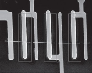
This scanning electron microscopy image shows three solar cells in series on a single nanowire with the core–shell regions outlined. (Image courtesy of Yang, et. al)
About a year ago, working with silicon, Yang and members of his research group developed a relatively inexpensive way to replace the planar p-n junctions of conventional solar cells with a radial p-n junction, in which a layer of n-type silicon formed a shell around a p-type silicon nanowire core. This geometry effectively turned each individual nanowire into a photovoltaic cell and greatly improved the light-trapping capabilities of silicon-based photovoltaic thin films.
Now they have applied this strategy to the fabrication of core/shell nanowires using cadmium sulfide and copper sulfide, but this time using solution chemistry. These core/shell nanowires were prepared using a solution-based cation (negative ion) exchange reaction that was originally developed by chemist Paul Alivisatos and his research group to make quantum dots and nanorods. Alivisatos is now the director of Berkeley Lab, and UC Berkeley’s Larry and Diane Bock Professor of Nanotechnology.
“The initial cadmium sulfide nanowires were synthesized by physical vapor transport using a vapor–liquid–solid (VLS) mechanism rather than wet chemistry, which gave us better quality material and greater physical length, but certainly they can also be made using solution process” Yang says. “The as-grown single-crystalline cadmium sulfide nanowires have diameters of between 100 and 400 nanometers and lengths up to 50 millimeters.”
The cadmium sulfide nanowires were then dipped into a solution of copper chloride at a temperature of 50 degrees Celsius and kept there for 5 to 10 seconds. The cation exchange reaction converted the surface layer of the cadmium sulfide into a copper sulfide shell.
“The solution-based cation exchange reaction provides us with an easy, low-cost method to prepare high-quality hetero-epitaxial nanomaterials,” Yang says. “Furthermore, it circumvents the difficulties of high-temperature doping and deposition for typical vapor phase production methods, which suggests much lower fabrication costs and better reproducibility. All we really need are beakers and flasks for this solution-based process. There’s none of the high fabrication costs associated with gas-phase epitaxial chemical vapor deposition and molecular beam epitaxy, the techniques most used today to fabricate semiconductor nanowires.”
Yang and his colleagues believe they can improve the energy conversion efficiency of their solar cell nanowires by increasing the amount of copper sulfide shell material. For their technology to be commercially viable, they need to reach an energy conversion efficiency of at least ten-percent.
This research was supported by the DOE Office of Science.
# # #
Lawrence Berkeley National Laboratory addresses the world’s most urgent scientific challenges by advancing sustainable energy, protecting human health, creating new materials, and revealing the origin and fate of the universe. Founded in 1931, Berkeley Lab’s scientific expertise has been recognized with 12 Nobel prizes. The University of California manages Berkeley Lab for the U.S. Department of Energy’s Office of Science. For more, visit www.lbl.gov.
Additional Information
For more about the research of Peidong Yang and his group, visit the Website at http://www.cchem.berkeley.edu/pdygrp/main.html