Contact: Lynn Yarris (510) 486-5375, [email protected]
BERKELEY, CA – Multiferroics are materials in which unique combinations of electric and magnetic properties can simultaneously coexist. They are potential cornerstones in future magnetic data storage and spintronic devices provided a simple and fast way can be found to turn their electric and magnetic properties on and off. In a promising new development, researchers with the U.S. Department of Energy’s Lawrence Berkeley National Laboratory (Berkeley Lab) working with a prototypical multiferroic have successfully demonstrated just such a switch — electric fields.

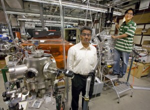
Ramamoorthy Ramesh and Chan-Ho Yang of Berkeley Lab’s Materials Sciences Division successfully demonstrated that electric fields can be used as ON/OFF switches in doped multiferroic films, a development that holds promise for future magnetic data storage and spintronic devices.
“Using electric fields, we have been able to create, erase and invert p-n junctions in a calcium-doped bismuth ferrite film,” said Ramamoorthy Ramesh of Berkeley Lab’s Materials Sciences Division (MSD), who led this research.
“Through the combination of electronic conduction with the electric and magnetic properties already present in the multiferroic bismuth ferrite, our demonstration opens the door to merging magnetoelectrics and magnetoelectronics at room temperature.”
Ramesh, who is also a professor in the Department of Materials Science and Engineering and the Department of Physics at UC Berkeley, has published a paper on this research that is now available in the on-line edition of the journal Nature Materials. The paper is titled: “Electric modulation of conduction in multiferroic Ca-doped BiFeO3 films.” Co-authoring the paper with Ramesh were Chan-Ho Yang, Jan Seidel,Sang-Yong Kim, Pim Rossen, Pu Yu, Marcin Gajek, Ying-Hao Chu, Lane Martin, Micky Holcomb, Qing He, Petro Maksymovych, Nina Balke, Sergei Kalinin, Arthur Baddorf, Sourav Basu and Matthew Scullin.
The next generation of computers promises to be smaller, faster and far more versatile than today’s devices thanks in part to the anticipated development of memory chips that store data through electron spin and its associated magnetic moment rather than electron charge. Because multiferroics simultaneously exhibit two or more ferro electric or magnetic properties in response to changes in their environment, they’re considered prime candidates to be the materials of choice for this technology.

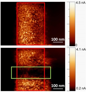
This image recorded after an electric field was applied to a calcium-doped bismuth ferrite multiferroic film shows in the top image current being conducted within the red rectangle (On). In the bottom image, an opposite electric field was applied to the area within the green rectangle, switching it back to an insulating state (Off).
Bismuth ferrite is a multiferroic comprised of bismuth, iron and oxygen (BiFeO3). It is both ferroelectric and antiferromagnetic (“ferro” refers to magnetism in iron but the term has grown to include materials and properties that have nothing to do with iron), and has commanded particular interest in the spintronics field, especially after a surprising discovery by Ramesh and his group earlier this year. They found that although bismuth ferrite is an insulating material, running through its crystals are ultrathin (two-dimensional) sheets called “domain walls” that conduct electricity at room temperature. This discovery suggested that with the right doping, the conducting states in bismuth ferrite could be stabilized, opening the possibility of creating p-n junctions, a crucial key to solid state electronics.
“Insulator to conductor transitions are typically controlled through the combination of chemical doping and magnetic fields but magnetic fields are too expensive and energy-consuming to be practical in commercial devices,” said Ramesh. “Electric fields are much more useful control parameters because you can easily apply a voltage across a sample and modulate it as needed to induce insulator-conductor transitions.”
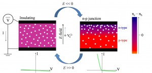
In their new study, Ramesh and his group first doped the bismuth ferrite with calcium acceptor ions, which are known to increase the amount of electric current that materials like bismuth ferrite can carry. The addition of the calcium ions created positively-charged oxygen vacancies. When an electric field was applied to the calcium-doped bismuth ferrite films, the oxygen vacancies became mobile. The electric field “swept” the oxygen vacancies towards the film’s top surface, creating an n-type semiconductor in that portion of the film, while the immobile calcium ions created a p-type semiconductor in the bottom portion. Reversing the direction of the electric field inverted the n-type and p-type semiconductor regions, and a moderate field erased them.
“It is the same principle as in a CMOS device where the application of a voltage serves as an on/off switch that controls electron transport properties and changes electrical resistance from high (insulator) to low (conductor),” said Ramesh.

This schematic diagram shows a calcium-doped bismuth ferrite multiferroic film existing in a highly insulating state until the application of an electric field mobilizes oxygen vacancies to create n- and p-type conductors in the top and bottom portions of the film respectively.
Whereas a typical CMOS device features an on/off switching ratio (the difference between resistance and non-resistance to electrical current) of about one million, Ramesh and his group achieved an on/off switching ratio of about a thousand in their calcium-doped bismuth ferrite films. While this ratio is sufficient for device operation and double the best ratio achieved with magnetic fields, Chan-Ho Yang, lead author on this Nature Materials paper and a post-doc in Ramesh’s group says it can be improved.
“To make the ON state more conductive, we have many ideas to try such as different calcium-doping ratios, different strain states, different growth conditions, and eventually different compounds using the same idea,” Yang said.
A year ago, Ramesh and his group demonstrated that an electric field could be used to control ferromagnetism in a non-doped bismuth ferrite film. (See Nature Materials, “Electric-field control of local ferromagnetism using a magnetoelectric multiferroic”)
With this new demonstration that the combination of doping and an applied electric field can change the insulating-conducting state of a multiferroic, he and his colleagues have shown one way forward in adapting multiferroics to such phenomena as colossal magnetoresistance, high temperature superconductivity and SQUID-type magnetic field detectors as well as spintronics.
Said Yang, “Oxides such as bismuth ferrite are abundant and display many exotic properties including high-temperature superconductivity and colossal magnetoresistance, but they have not been used much in real applications because it has been so difficult to control defects, especially, oxygen vacancies. Our observations suggest a general technique to make oxygen vacancy defects controllable.”
Much of the work in this latest study by Ramesh and his group was carried out at Berkeley Lab’s Advanced Light Source (ALS), on the PEEM2 microscope. PEEM, which stands for PhotoEmission Electron Microscopy, is an ideal technique for studying ferro magnetic and antimagnetic domains, and PEEM2, powered by a bend magnet at ALS beamline 7.3.1.1, is one of the world’s best instruments, able to resolve features only a few nanometers thick.
“Without the capabilities of PEEM2 our experiments would have been dead in the water,” said Ramesh. “Andreas Scholl (who manages PEEM2) and his ALS team were an enormous help.”
This research was primarily supported by the U.S. Department of Energy’s Office of Science through its Basic Energy Sciences program.
Berkeley Lab is a U.S. Department of Energy national laboratory located in Berkeley, California. It conducts unclassified scientific research and is managed by the University of California.
Additional Information:
For more information on the research of Ramamoorthy Ramesh, visit his Website at http://www.lbl.gov/msd/investigators/investigators_all/ramesh_investigator.html