Contact: Paul Preuss, (510) 486-6249

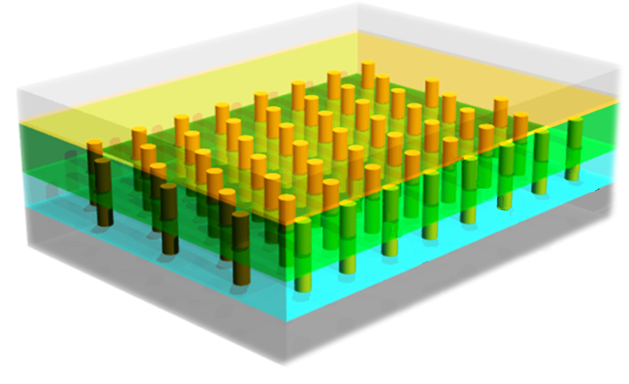
An aluminum substrate forms a template for a forest of cadmium sulfide nanopillars and also serves as a bottom electrode. Embedded in clear cadmium telluride and equipped with a top electrode of copper and gold, the result is an inexpensive and efficient 3-D solar cell.
BERKELEY, CA – Researchers at the U.S. Department of Energy’s Lawrence Berkeley National Laboratory and the University of California at Berkeley have demonstrated a way to fabricate efficient solar cells from low-cost and flexible materials. The new design grows optically active semiconductors in arrays of nanoscale pillars, each a single crystal, with dimensions measured in billionths of a meter.
“To take advantage of abundant solar energy we have to find ways to mass-produce efficient photovoltaics,” says Ali Javey, a faculty scientist in Berkeley Lab’s Materials Sciences Division and a professor of electrical engineering and computer science at UC Berkeley. “Single-crystalline semiconductors offer a lot of promise, but standard ways of making them aren’t economical.”
A solar cell’s basic job is to convert light energy into charge-carrying electrons and “holes” (the absence of an electron), which flow to electrodes to produce a current. Unlike a typical two-dimensional solar cell, a nanopillar array offers much more surface for collecting light. Computer simulations have indicated that, compared to flat surfaces, nanopillar semiconductor arrays should be more sensitive to light, have a greatly enhanced ability to separate electrons from holes, and be a more efficient collector of these charge carriers.
“Unfortunately, early attempts to make photovoltaic cells based on pillar-shaped semiconductors grown from the bottom up yielded disappointing results. Light-to-electricity efficiencies were less than one to two percent,” says Javey. “Epitaxial growth on single crystalline substrates was often used, which is costly. The nanopillar dimensions weren’t well controlled, pillar density and alignment was poor, and the quality of the interface between the semiconductors was poor.”
Javey devised a new, controlled way to use a method called the “vapor-liquid-solid” process to make large-scale modules of dense, highly ordered arrays of single-crystal nanopillars. Inside a quartz furnace his group grew pillars of electron-rich cadmium sulfide on aluminum foil, in which geometrically distributed pores made by anodization served as a template.
In the same furnace they submerged the nanopillars, once grown, in a thin layer of hole-rich cadmium telluride, which acted as a window to collect the light. The two materials in contact with each other form a solar cell in which the electrons flow through the nanopillars to the aluminum contact below, and the holes are conducted to thin copper-gold electrodes placed on the surface of the window above.
The efficiency of the test device was measured at six percent, which while less than the 10 to 18 percent range of mass-produced commercial cells is higher than most photovoltaic devices based on nanostructured materials – even though the nontransparent copper-gold electrodes on top of the Javey group’s test device cut its efficiency by 50 percent. In future, top contact transparency can easily be improved.
Other factors that greatly affect the efficiency of a 3-D nanopillar-array solar cell include its density and the exposed length of the pillars in contact with the window material. These dimensions are easily optimized in future generations of the device.

A flexible solar cell is achieved by removing the aluminum substrate, substituting an indium bottom electrode, and embedding the 3-D array in clear plastic.
Concerned with practical applications as well as theoretical performance, the researchers made a flexible solar cell of the same design by etching away the aluminum substrate and substituting a thin layer of indium for the bottom electrode. They sheathed the whole solar cell in clear plastic (polydimethylsiloxane) to make a bendable device, which could be flexed with only marginal effect on performance – and no degradation of performance after repeated bending.
“There are lots of ways to improve 3-D nanopillar photovoltaics for higher performance, and ways to simplify the fabrication process as well, but the method is already hugely promising as a way to lower the cost of efficient solar cells,” says Javey. “There’s the ability to grow single-crystalline structures directly on large aluminum sheets. And the 3-D configuration means the requirements for quality and purity of the input materials are less stringent and less costly. Nanopillar arrays are a new path to versatile solar modules.”
“Three-dimensional nanopillar-array photovoltaics on low-cost and flexible substrates,” by Zhiyong Fan, Haleh Razavi, Jae-won Do, Aimee Moriwaki, Onur Ergen, Yu-Lun Chueh, Paul W. Leu, Johhny C. Ho, Toshitake Takahashi, Lothar A. Reichertz, Steven Neale, Kyoungsik Yu, Ming Wu, Joel W. Ager, and Ali Javey, appears in the August issue of Nature Materials and is available in advance online publication at http://www.nature.com/nmat/journal/vaop/ncurrent/abs/nmat2493.html.
This work was supported in part by the Helios Solar Energy Research Center, which is supported by the U.S. Department of Energy’s Office of Science, Office of Basic Energy Sciences.
Berkeley Lab is a U.S. Department of Energy national laboratory located in Berkeley, California. It conducts unclassified scientific research and is managed by the University of California. Visit our website at http://www.lbl.gov.