Scientific contact: Michael Crommie, 510-642-9392

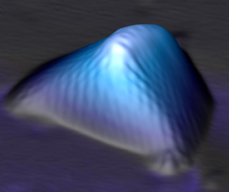
In this scanning tunneling microscopy image of a graphene nanobubble, the hexagonal two-dimensional graphene crystal is seen distorted and stretched along three main axes. The strain creates pseudo-magnetic fields far stronger than any magnetic field ever produced in the laboratory. (Click on images for best resolution.)
Graphene, the extraordinary form of carbon that consists of a single layer of carbon atoms, has produced another in a long list of experimental surprises. In the July 30, 2010 issue of the journal Science, a multi-institutional team of researchers headed by Michael Crommie, a faculty senior scientist in the Materials Sciences Division at the U.S. Department of Energy’s Lawrence Berkeley National Laboratory and a professor of physics at the University of California at Berkeley, reports the creation of pseudo-magnetic fields far stronger than the strongest magnetic fields ever sustained in a laboratory – just by putting the right kind of strain onto a patch of graphene.
“We have shown experimentally that when graphene is stretched to form nanobubbles on a platinum substrate, electrons behave as if they were subject to magnetic fields in excess of 300 tesla, even though no magnetic field has actually been applied,” says Crommie. “This is a completely new physical effect that has no counterpart in any other condensed matter system.”
Crommie notes that “for over 100 years people have been sticking materials into magnetic fields to see how the electrons behave, but it’s impossible to sustain tremendously strong magnetic fields in a laboratory setting.” The current record is 85 tesla for a field that lasts only thousandths of a second. When stronger fields are created, the magnets blow themselves apart.
The ability to make electrons behave as if they were in magnetic fields of 300 tesla or more – just by stretching graphene – offers a new window on a source of important applications and fundamental scientific discoveries going back over a century. This is made possible by graphene’s electronic behavior, which is unlike any other material’s.
A carbon atom has four valence electrons; in graphene (and in graphite, a stack of graphene layers), three electrons bond in a plane with their neighbors to form a strong hexagonal pattern, like chicken-wire. The fourth electron sticks up out of the plane and is free to hop from one atom to the next. The latter pi-bond electrons act as if they have no mass at all, like photons. They can move at almost one percent of the speed of light.
The idea that a deformation of graphene might lead to the appearance of a pseudo-magnetic field first arose even before graphene sheets had been isolated, in the context of carbon nanotubes (which are simply rolled-up graphene). In early 2010, theorist Francisco Guinea of the Institute of Materials Science of Madrid and his colleagues developed these ideas and predicted that if graphene could be stretched along its three main crystallographic directions, it would effectively act as though it were placed in a uniform magnetic field. This is because strain changes the bond lengths between atoms and affects the way electrons move between them. The pseudo-magnetic field would reveal itself through its effects on electron orbits.
In classical physics, electrons in a magnetic field travel in circles called cyclotron orbits. These were named following Ernest Lawrence’s invention of the cyclotron, because cyclotrons continuously accelerate charged particles (protons, in Lawrence’s case) in a curving path induced by a strong field.
Viewed quantum mechanically, however, cyclotron orbits become quantized and exhibit discrete energy levels. Called Landau levels, these correspond to energies where constructive interference occurs in an orbiting electron’s quantum wave function. The number of electrons occupying each Landau level depends on the strength of the field – the stronger the field, the more energy spacing between Landau levels, and the denser the electron states become at each level – which is a key feature of the predicted pseudo-magnetic fields in graphene.
A serendipitous discovery
Describing their experimental discovery, Crommie says, “We had the benefit of a remarkable stroke of serendipity.”

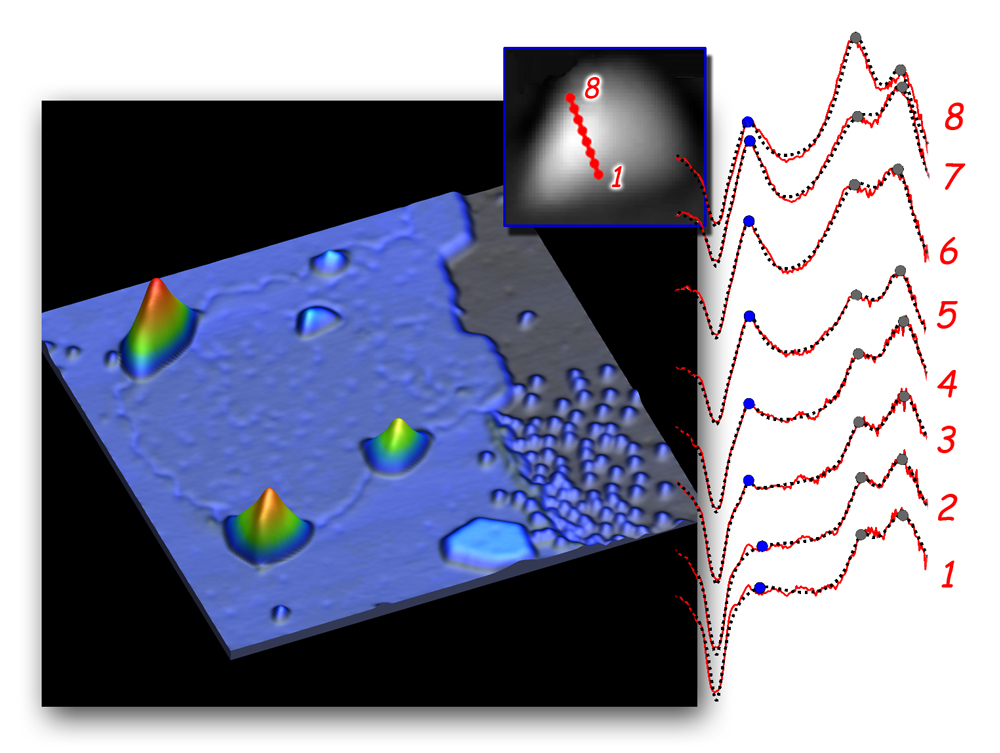
A patch of graphene at the surface of a platinum substrate exhibits four triangular nanobubbles at its edges and one in the interior. Scanning tunneling spectroscopy taken at intervals across one nanobubble (inset) shows local electron densities clustering in peaks at discrete Landau-level energies. Pseudo-magnetic fields are strongest at regions of greatest curvature.
Crommie’s research group had been using a scanning tunneling microscope to study graphene monolayers grown on a platinum substrate. A scanning tunneling microscope works by using a sharp needle probe that skims along the surface of a material to measure minute changes in electrical current, revealing the density of electron states at each point in the scan while building an image of the surface.
Crommie was meeting with a visiting theorist from Boston University, Antonio Castro Neto, about a completely different topic when a group member came into his office with the latest data.
“It showed nanobubbles, little pyramid-like protrusions, in a patch of graphene on the platinum surface,” Crommie says, “and associated with the graphene nanobubbles there were distinct peaks in the density of electron states.”
Crommie says his visitor, Castro Neto, took one look and said, “That looks like the Landau levels predicted for strained graphene.”
Sure enough, close examination of the triangular bubbles revealed that their chicken-wire lattice had been stretched precisely along the three axes needed to induce the strain orientation that Guinea and his coworkers had predicted would give rise to pseudo-magnetic fields. The greater the curvature of the bubbles, the greater the strain, and the greater the strength of the pseudo-magnetic field. The increased density of electron states revealed by scanning tunneling spectroscopy corresponded to Landau levels, in some cases indicating giant pseudo-magnetic fields of 300 tesla or more.
“Getting the right strain resulted from a combination of factors,” Crommie says. “To grow graphene on the platinum we had exposed the platinum to ethylene” – a simple compound of carbon and hydrogen – “and at high temperature the carbon atoms formed a sheet of graphene whose orientation was determined by the platinum’s lattice structure.”
To get the highest resolution from the scanning tunneling microscope, the system was then cooled to a few degrees above absolute zero. Both the graphene and the platinum contracted – but the platinum shrank more, with the result that excess graphene pushed up into bubbles, measuring four to 10 nanometers (billionths of a meter) across and from a third to more than two nanometers high.

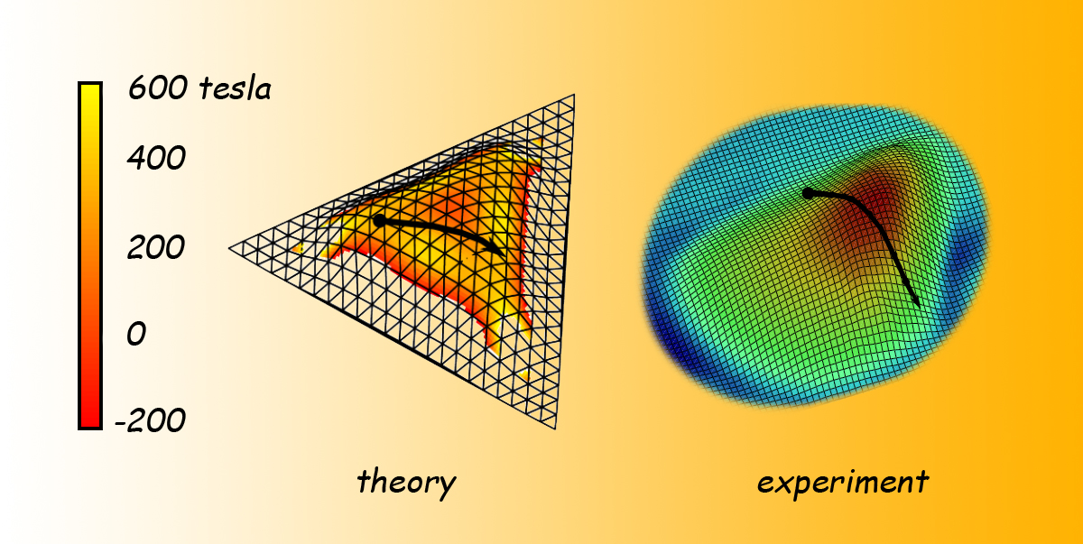
The colors of a theoretical model of a nanobubble (left) show that the pseudo-magnetic field is greatest where curvature, and thus strain, is greatest. In a graph of experimental observations (right), colors indicate height, not field strength, but measured field effects likewise correspond to regions of greatest strain and closely match the theoretical model.
To confirm that the experimental observations were consistent with theoretical predictions, Castro Neto worked with Guinea to model a nanobubble typical of those found by the Crommie group. The resulting theoretical picture was a near-match to what the experimenters had observed: a strain-induced pseudo-magnetic field some 200 to 400 tesla strong in the regions of greatest strain, for nanobubbles of the correct size.
“Controlling where electrons live and how they move is an essential feature of all electronic devices,” says Crommie. “New types of control allow us to create new devices, and so our demonstration of strain engineering in graphene provides an entirely new way for mechanically controlling electronic structure in graphene. The effect is so strong that we could do it at room temperature.”
The opportunities for basic science with strain engineering are also huge. For example, in strong pseudo-magnetic fields electrons orbit in tight circles that bump up against one another, potentially leading to novel electron-electron interactions. Says Crommie, “this is the kind of physics that physicists love to explore.”
“Strain-induced pseudo-magnetic fields greater than 300 tesla in graphene nanobubbles,” by Niv Levy, Sarah Burke, Kacey Meaker, Melissa Panlasigui, Alex Zettl, Francisco Guinea, Antonio Castro Neto, and Michael Crommie, appears in the July 30, 2010 issue of Science and is available online to subscribers. The work was supported by the Department of Energy’s Office of Science and by the Office of Naval Research.
Additional information
Lawrence Berkeley National Laboratory provides solutions to the world’s most urgent scientific challenges including clean energy, climate change, human health, novel materials, and a better understanding of matter and force in the universe. It is a world leader in improving our lives and knowledge of the world around us through innovative science, advanced computing, and technology that makes a difference. Berkeley Lab is a U.S. Department of Energy (DOE) national laboratory managed by the University of California for the DOE Office of Science. Visit our website.