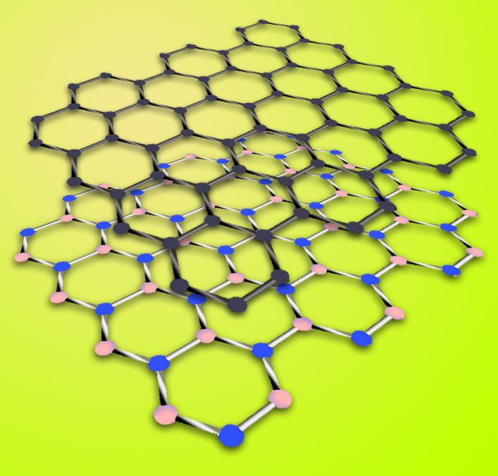
Graphene (top layer) is a hexagonal arrangement of carbon atoms. Hexagonal boron nitride is a similar arrangement of boron and nitrogen atoms whose lattice constant is just 1.7 percent larger. Boron nitride’s attributes make it an excellent substrate for preserving graphene’s intrinsic properties.
Graphene is a two-dimensional honeycomb of carbon, just one atom thick, whose intriguing electronic properties include very high electron mobility and very low resistivity. Graphene is so sensitive to its environment, however, that these remarkable attributes can be wrecked by interference from nearby materials. Finding the best substrate on which to mount graphene is critical if graphene devices are ever to become practical.
Groups led by Michael Crommie and Alex Zettl, scientists in the Materials Sciences Division at the U.S. Department of Energy’s Lawrence Berkeley National Laboratory (Berkeley Lab) and professors of physics at the University of California at Berkeley, have joined forces to examine the best substrate candidates for preserving graphene’s intrinsic properties. Results of their research on graphene’s interaction with a boron nitride substrate recently appeared in Nano Letters.
“Any substrate influences the properties of graphene, so if you want to study its intrinsic properties the best way is to work with suspended graphene,” says Régis Decker, a former postdoctoral fellow in the Crommie group, now at the University of Hamburg, Germany, and lead author of the Nano Letters report. “However, suspended graphene is quite unstable when investigated with scanning probe techniques like scanning tunneling microscopy” – STM – “because the graphene membrane can vibrate under the tip. So the idea is to find a substrate that mimics the case of suspended graphene.”
A group based at Columbia University reported, in October 2010, that graphene supported on a boron nitride (BN) substrate had dramatically better electron mobility than graphene mounted on the most common semiconductor substrate, silicon dioxide (SiO2).
“The Columbia group showed that the mobility of electrons in graphene on boron nitride is much better than graphene on silicon dioxide, but there were many questions that their macroscopic measurements didn’t answer,” says the Crommie group’s Yang Wang, co-lead author of the Nano Letters report. The Crommie and Zettl groups compared the two systems side by side to find out just why boron nitride works so well. “To investigate BN on the atomic scale we used STM to build up a picture of the topography of the system and measure its local electronic states.”
Searching for what makes boron nitride special
Says Decker, “For a graphene-substrate system to be able to mimic suspended graphene, the substrate needs a large electronic band gap and no dangling bonds, so as to avoid any change in the electronic structure of graphene. The substrate would also need to be very flat, as suspended graphene would be. Boron nitride is a good candidate because it fills these requirements.”
What first attracted investigators to boron nitride’s potential as a graphene substrate were its unusual structural properties. In its hexagonal structure (h-BN), alternating nitrogen and boron atoms closely mimic the way carbon atoms are arranged in graphene. Boron and nitrogen atoms in BN compounds are paired equally, and together their valence electrons (three and five, respectively) equal those of a pair of carbon atoms (four each). Although the h-BN lattice is some 1.7 percent larger than graphene’s and not commensurate with it, the two honeycombs laid one on the other can be aligned much more closely than graphene on silicon dioxide. Unlike graphene, which normally has no band gap, h-BN has a wide band gap, due to the alternating boron and nitrogen atoms in its lattice.

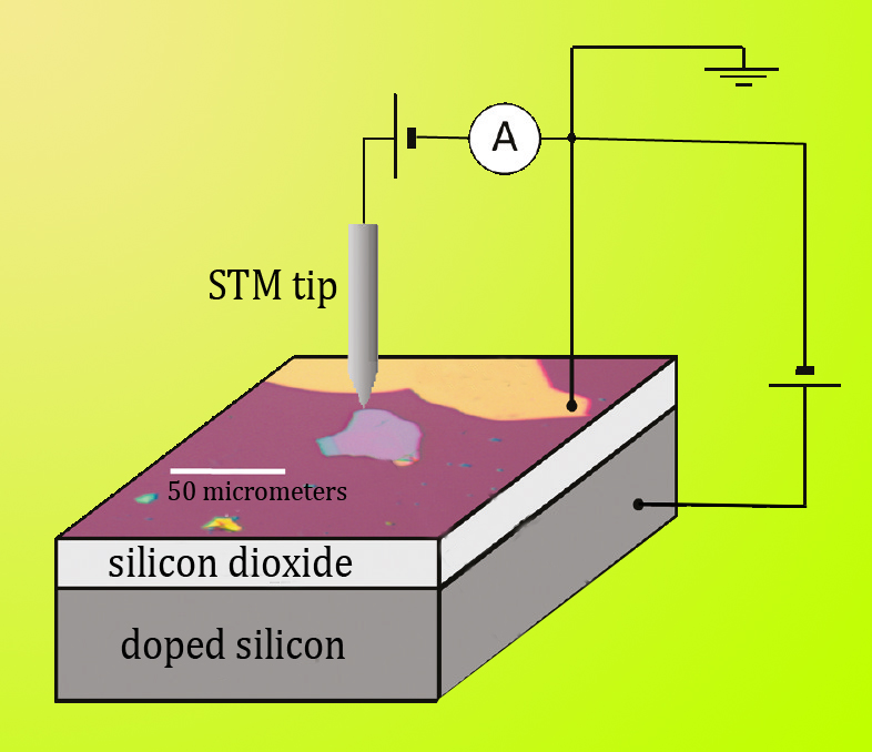
The researchers deposited boron nitride flakes on a layer of silicon dioxide, grown on a layer of doped silicon. The doped silicon was used as a gate electrode for doping the graphene during scanning tunneling microscopy. Graphene was applied to both the boron nitride flakes (under the STM tip) and the bare silicon dioxide; the graphene (dark and light purple) was grounded by an electrode of gold/titanium (gold). The STM could scan across both substrate systems.
To create graphene/BN devices, the Zettl group first reduced boron nitride crystals to tiny flakes by the tried-and-true method of “exfoliating” them between strips of Scotch Tape. The BN flakes were deposited on a layer of SiO2, which was grown on a layer of doped silicon which, in turn, was used as a gate electrode to tune the charge concentration – a way of “doping” the graphene layer above – during scanning tunneling microscopy.
The Crommie group’s Qiong Wu created graphene by means of chemical vapor deposition on copper; on copper, carbon atoms self-assemble into a honeycomb lattice a single atom thick. The graphene sheets were transferred from the copper to soft plastic and then placed on top of the boron nitride flakes by pressing the plastic onto the BN. The whole assembly was annealed at high heat.
The graphene layer was grounded by depositing a titanium gold electrode on it. Three graphene/BN systems were made this way, ready for direct STM comparisons with graphene on silicon dioxide. The STM tip could scan across the graphene layer, measuring topography and local charge concentrations at various doping levels determined by the silicon-layer gate electrode.
Boron nitride versus silicon dioxide
“A couple of things were thought to interfere with electron mobility in graphene on silicon dioxide,” says Victor Brar of the Crommie group. “One is impurities that dope the graphene and locally alter the concentration of charges.”
A sure way to shorten the mean free path of electrons (or their positively charged counterparts, electron absences called holes) is to strew the path with obstacles known as charge puddles, which are fluctuations in local concentrations of charge. In graphene on SiO2, charge puddles are common.
“We had previously studied the properties of graphene/silicon dioxide systems in detail,” says Michael Crommie, “and showed that charge puddles aren’t caused by ripples or corrugations in the graphene sheet, as had been suggested, but rather by impurities below the graphene layer.”
One source of those impurities could be foreign matter trapped between the graphene and the substrate when the graphene layer is applied. Tiny air bubbles or water molecules or other foreign matter could act as dopants.
“When we made the graphene on boron-nitride devices we looked for atmospheric impurities, but we didn’t see any evidence of their effects,” says Brar. “For making practical graphene devices, that’s good news, because it means they don’t have to be assembled in a vacuum.”

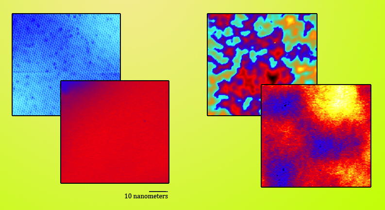
Results of measuring graphene on a boron nitride substrate are at left, graphene on silicon dioxide at right. The STM mapped both the topography of the systems (back) and the local charge densities (front). Graphene on boron nitride is extraordinarily flat, and inhomogeniety of local charge states is signicantly reduced compared to silicon dioxide.
Another source of graphene doping and subsequent charge concentrations is dangling bonds in the substrate. A valence electron available for bonding with another atom is a recipe for chemical reactivity, and silicon dioxide has a high concentration of dangling bonds. Boron nitride, however, has no leftover electrons to form dangling bonds.
STM comparisons of the two systems vividly displayed the differences between them. Topographically, graphene on boron nitride is much less rough than graphene on silicon, with height differences on the scanned surfaces reaching only around 40 picometers (trillionths of a meter). Height differences with the silicon dioxide substrate were up to 30 times greater.
Electronically, variations in charge density were reduced dramatically in the BN substrate. Compared to the nearly unvarying values of the boron nitride system, graphs of the silicon dioxide systems resemble modern-art color-field paintings.
Finally, Decker says, “because its lattice constant is very close to that of graphene, theorists predicted that this induces a band gap in graphene, which would be interesting for applications” – if not for maintaining graphene’s intrinsic properties. The Crommie group investigated how electronic properties might vary according to the orientation of the graphene sheet on the boron nitride substrate. The two, not-quite-commensurate lattices betrayed their alignment by exhibiting changing moiré patterns with different orientations.
Says Wang, “We saw many different alignments, including alignments that were almost perfect. But the graphene still showed no band gap.” In sum, how graphene is oriented on a boron nitride substrate makes no detectable difference in its excellent electronic properties.
Michael Crommie says, “The graphene/BN system is really much nicer than any other substrate for a range of applications. There are many fewer impurities, much less charge inhomogeneity, much less bumpiness, and much more stability – in all, a much cleaner environment for studying graphene’s intrinsic properties. Boron nitride is a really fabulous system for practical graphene devices.”
More information
“Local electronic properties of graphene on a BN substrate via scanning tunneling microscopy,” by Régis Decker, Yang Wang, Victor W. Brar, William Regan, Hsin-Zon Tsai, Qiong Wu, William Gannett, Alex Zettl, and Michael F. Crommie, appears in Nano Letters and is available online at http://pubs.acs.org/doi/abs/10.1021/nl2005115.
After the Crommie and Zettl groups submitted their paper, related work by Xue et al appeared in Nature Materials, April 2011, available online at http://www.nature.com/nmat/journal/v10/n4/abs/nmat2968.html.
Early results measuring the properties of graphene on a boron nitride substrate were published by Dean et al in Nature Nanotechnology, October 2010, available online at http://www.nature.com/nnano/journal/v5/n10/abs/nnano.2010.172.html