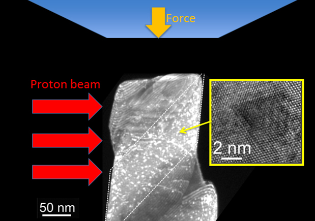
Scientists at Lawrence Berkeley National Laboratory and the University of California at Berkeley conducted compression tests of copper specimens irradiated with high-energy protons, designed to model how damage from radiation affects the mechanical properties of copper. By using a specialized in situ mechanical testing device in a transmission electron microscope at the National Center for Electron Microscopy, the team could examine — with nanoscale resolution — the localized nature of this deformation. (Scales in nanometers, billionths of a meter)
Nuclear power is a major component of our nation’s long-term clean-energy future, but the technology has come under increased scrutiny in the wake of Japan’s recent Fukushima disaster. Indeed, many nations have called for checks and “stress tests” to ensure nuclear plants are operating safely.
In the United States, about 20 percent of our electricity and almost 70 percent of the electricity from emission-free sources, including renewable technologies and hydroelectric power plants, is supplied by nuclear power. Along with power generation, many of the world’s nuclear facilities are used for research, materials testing, or the production of radioisotopes for the medical industry. The service life of structural and functional material components in these facilities is therefore crucial for ensuring reliable operation and safety.
Now scientists at Berkeley Lab, the University of California at Berkeley, and Los Alamos National Laboratory have devised a nanoscale testing technique for irradiated materials that provides macroscale materials-strength properties under certain conditions. This technique could help accelerate the development of new materials for nuclear applications and provide insights on ways to reduce the amount of material required for testing of facilities already in service.
“Nanoscale mechanical tests always give you higher strengths than the macroscale, bulk values for a material. This is a problem if you actually want to use a nanoscale test to tell you something about the bulk-material properties,” said Andrew Minor, a faculty scientist in the National Center for Electron Microscopy (NCEM) and an associate professor in the materials science and engineering department at UC Berkeley. “We have shown you can actually get real properties from irradiated specimens as small as 400 nanometers in diameter, which may provide new avenues for the field of nuclear materials to take advantage of nanoscale testing.”
In this study, Minor and his colleagues conducted compression tests of copper specimens irradiated with high-energy protons, designed to model how damage from radiation affects the mechanical properties of copper. By using a specialized in situ mechanical testing device in a transmission electron microscope at NCEM, the team could examine — with sub-nanoscale resolution — the nature of the deformation and how it was localized to just a few atomic planes.

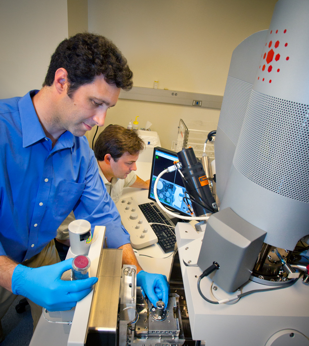
Berkeley Lab scientist Andy Minor (left) and Peter Hosemann have devised a nanoscale testing technique for irradiated materials to provide macroscale materials-strength properties. This technique could help accelerate the development of new materials for nuclear applications, while reducing the amount of material required for testing facilities already in service. (Click on image for best resolution.)
Three-dimensional defects within the copper created by radiation can block the motion of one-dimensional defects in the crystal structure, called dislocations. This interaction causes irradiated materials to become brittle, and alters the amount of force a material can withstand before it eventually breaks. Additionally, the complex microstructures resulting from irradiation may result in dislocation interactions in nanoscale samples that have the same effects on strength as in bulk materials. By translating nanoscale strength values into bulk properties, this technique could help reactor designers find suitable materials for engineering components in nuclear plants.
“This small-scale testing technique could help extend the lifetime of a nuclear reactor,” said co-author Peter Hosemann, an assistant professor in the nuclear engineering department at UC Berkeley. “By using a smaller specimen, we limit any safety issues related to the handling of the test material and could potentially measure the exact properties of a material already being used in a 40-year-old nuclear facility to make sure this structure lasts well into the future.”
Minor adds, “Understanding how materials fail is a fundamental mechanistic question. This proof of principle study gives us a model system from which we can now start to explore real, practical materials applicable to nuclear energy. By understanding the role of defects on the mechanical properties of nuclear reactor materials, we can design materials that are more resistant to radiation damage, leading to more advanced and safer nuclear technologies.”
A paper reporting this research titled, “In situ nanocompression testing of irradiated copper,” appears in Nature Materials and is available to subscribers online. Co-authoring the paper with Minor and Hosemann were Daniel Kiener and Stuart Maloy. Portions of this work at the National Center for Electron Microscopy were supported by DOE’s Office of Science.
Lawrence Berkeley National Laboratory addresses the world’s most urgent scientific challenges by advancing sustainable energy, protecting human health, creating new materials, and revealing the origin and fate of the universe. Founded in 1931, Berkeley Lab’s scientific expertise has been recognized with 12 Nobel prizes. The University of California manages Berkeley Lab for the U.S. Department of Energy’s Office of Science. For more, visit www.lbl.gov.