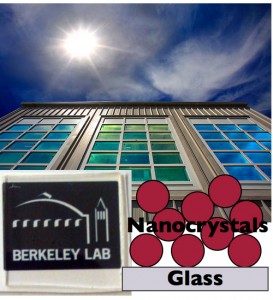
Berkeley Lab researchers have unveiled a semiconductor nanocrystal coating material capable of controlling heat from the sun while remaining transparent. This heat passes through the film without affecting its visible transmittance, which could add a critical energy-saving dimension to “smart window” coatings.
Researchers with the U.S. Department of Energy (DOE)’s Lawrence Berkeley National Laboratory (Berkeley Lab) have unveiled a semiconductor nanocrystal coating material capable of controlling heat from the sun while remaining transparent. Based on electrochromic materials, which use a jolt of electric charge to tint a clear window, this breakthrough technology is the first to selectively control the amount of near infrared radiation. This radiation, which leads to heating, passes through the film without affecting its visible transmittance. Such a dynamic system could add a critical energy-saving dimension to “smart window” coatings.
“To have a transparent electrochromic material that can change its transmittance in the infrared portion of sunlight is completely unprecedented,” says Delia Milliron, director of the Inorganic Nanostructures Facility with Berkeley Lab’s Molecular Foundry, who led this research. “What’s more, the coloration efficiency of our material—a figure of merit describing the amount of current needed to make this thing go—is substantially higher than standard electrochromic materials, which means it’s also very efficient.”
Dynamic window coatings could translate into significant energy savings in buildings, which account for more than 40 percent of carbon emissions in the United States. According to studies conducted at the National Renewable Energy Laboratory, smart window coatings could offset the use of climate control and illumination systems by up to 49 percent for air conditioning and 51 percent for lighting.
“Traditional electrochromic windows cannot selectively control the amount of visible and near infrared light that transmits through the film. When operated, these windows can either block both regions of light or let them in simultaneously,” says Guillermo Garcia, a graduate student researcher at the Foundry. “This work represents a stepping stone to the ideal smart window, which would be able to selectively choose which region of sunlight is needed to optimize the temperature inside a building.”
To generate this new coating, the team developed a nanocrystal film of electrically doped indium tin oxide, a transparent semiconductor typically used as a conductive coating for flat screen TVs. By manipulating the electrons within this semiconducting film, they could tune the collective oscillations of these electrons—a phenomenon called plasmonics—across the near-infrared frequency range.

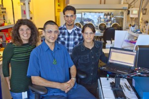
Berkeley Lab researchers (left to right) Raffaella Buonsanti, Rueben Mendelsberg, Guillermo Garcia and Delia Milliron have discovered a semiconductor nanocrystal coating material based on electrochromic materials, which use a jolt of electric charge to tint a clear window. This breakthrough technology is the first to selectively control the amount of near infrared radiation from the sun, which leads to heating. (Photo by Roy Kaltschmidt)
“Our ability to leverage plasmons in doped semiconductors with a very sensitive switching response in the near-infrared region also brings to mind applications in telecommunications,” Milliron adds. “We’ve also brought this synthesis into WANDA, our nanocrystal robot, which means we will be able to provide materials for a wide variety of user projects. “
“This work expands the versatility of electrochromic devices, opening up a variety of new applications in solar and thermal control,” says co-author Thomas Richardson, a staff scientist in Berkeley Lab’s Environmental and Energy Technologies Division. “The innovative mechanism with high coloration efficiency offers hope for improved switching ranges and long term durability.”
Garcia is the lead author and Milliron the corresponding author of a paper reporting this research in the journal Nano Letters. The paper is titled “Dynamically modulating the surface plasmon resonance of doped semiconductor nanocrystals.” Co-authoring the paper with Garcia, Milliron and Richardson were Raffaella Buonsanti, Evan Runnerstrom, Rueben Mendelsberg, Anna Llordes and Andre Anders.
This work at the Molecular Foundry was supported by DOE’s Office of Science.
The Molecular Foundry is one of the five DOE Nanoscale Science Research Centers (NSRCs), national user facilities for interdisciplinary research at the nanoscale, supported by the DOE Office of Science. Together the NSRCs comprise a suite of complementary facilities that provide researchers with state-of-the-art capabilities to fabricate, process, characterize and model nanoscale materials, and constitute the largest infrastructure investment of the National Nanotechnology Initiative. The NSRCs are located at DOE’s Argonne, Brookhaven, Lawrence Berkeley, Oak Ridge and Sandia and Los Alamos National Laboratories. For more information about the DOE NSRCs, please visit http://science.energy.gov.
###
Lawrence Berkeley National Laboratory addresses the world’s most urgent scientific challenges by advancing sustainable energy, protecting human health, creating new materials, and revealing the origin and fate of the universe. Founded in 1931, Berkeley Lab’s scientific expertise has been recognized with 12 Nobel prizes. The University of California manages Berkeley Lab for the U.S. Department of Energy’s Office of Science. For more, visit www.lbl.gov.
Additional Information
For more information about the Molecular Foundry visit the Website at http://foundry.lbl.gov/