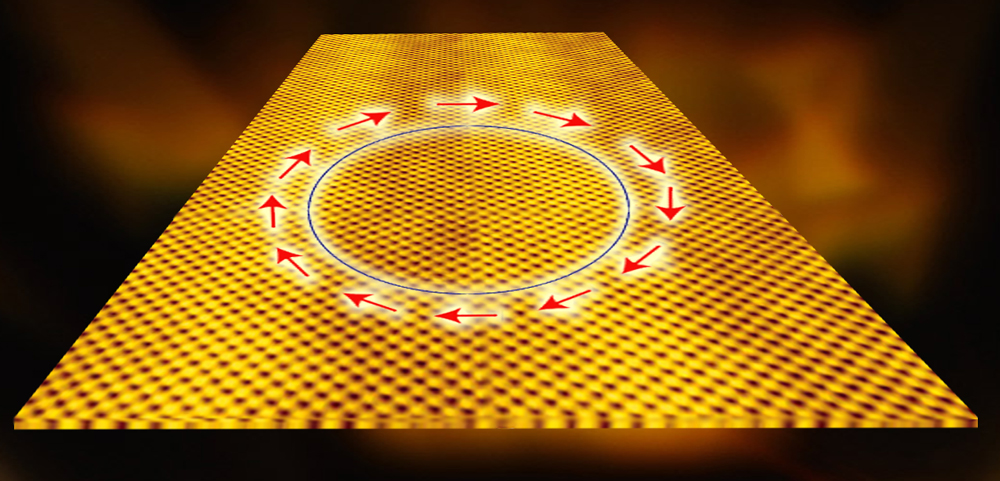
Electrons on the surface of a topological insulator can flow with little resistance. Their spin and direction are intimately related; the direction of the electron determines its spin and in turn is determined by it.
Strange new materials experimentally identified just a few years ago are now driving research in condensed-matter physics around the world. First theorized and then discovered by researchers at the U.S. Department of Energy’s Lawrence Berkeley National Laboratory (Berkeley Lab) and their colleagues in other institutions, these “strong 3-D topological insulators” – TIs for short – are seemingly mundane semiconductors with startling properties. For starters, picture a good insulator on the inside that’s a good conductor on its surface – something like a copper-coated bowling ball.
A topological insulator’s surface is not an ordinary metal, however. The direction and spin of the surface electrons are locked together and change in concert. And perhaps the most surprising prediction is that the surface electrons cannot be scattered by defects or other perturbations and thus meet little or no resistance as they travel. In the jargon, the surface states remain “topologically protected” – they can’t scatter without breaking the rules of quantum mechanics.
“One way that electrons lose mobility is by scattering on phonons,” says Alexei Fedorov, staff scientist for beamline 12.0.1 of Berkeley Lab’s Advanced Light Source (ALS). Phonons are the quantized vibrational energy of crystalline materials, treated mathematically as particles. “Our recent work on a particularly promising topological insulator shows that its surface electrons hardly couple with phonons at all. So there’s no impediment to developing this TI for spintronics and other applications.”
In a topological insulator motion and spin (not the classical spin of a top but a quantum measure of angular momentum) are locked together: the path of a TI’s surface electrons determines their spin and in turn is determined by it.
What difference does it make whether an electron is spin “up” or spin “down”? For one thing, electron spin is equivalent to magnetic orientation. Since the 1997 advent of computer hard-drives using spin-determined giant magnetoresistive read-write heads, data density has multiplied by scores. Magnetic random access memory chips, introduced in 2006, can read and write in nanoseconds and have unlimited endurance, ideal for satellite communications, vehicle data recorders, and industrial controls. Computer hard-drives with no moving parts have not been far behind, with spintronics promising rapidly improving capacity and dependability. Among other technologies on the horizon are batteries than can store and convert magnetic energy directly to spin-polarized electric current.
It now appears topological insulators may solve problems, not just make new gadgets. The “glass” that gives your smart phone or tablet its touchscreen, unlike ordinary glass, is not only transparent but conducts electricity. Currently it’s made of tin and indium, an increasly scarce resource. Bismuth selenide to the rescue: recently transparent electrodes were demonstrated that are transparent, heat and chemical resistant, and flexible as well.
The TI in question is bismuth selenide, Bi2Se3, on whose surface electrons can flow at room temperature, making it an attractive candidate for practical applications like spintronics devices, plus farther-out ones like quantum computers. Much of the research on electron-phonon coupling in Bi2Se3 was conducted at beamline 12.0.1 by a team including Fedorov, led by Tonica Valla of Brookhaven National Laboratory. Their results are reported in Physical Review Letters.
The right tool for the job
To study a TI’s surface conductivity, electron transport on its surface has to be separated from total conductivity, including the poorly conducting bulk. One experimental technique, called angle-resolved photoemission spectrometry (ARPES), is adept at doing just this.
ARPES shines bright light, like that produced by the Advanced Light Source, on a sample and captures the electrons that the energetic photons knock free. By recording the angle and energy of these photoemitted electrons on a CCD detector, ARPES gradually builds up a direct graphic visualization of the sample’s electronic structure.
“Of the several ARPES beamlines at the ALS, beamline 12.0.1 seems to have an ideal balance of energy, resolution, and flux for research on topological insulators,” says Fedorov. “This beamline was used for some of the first experiments establishing that 3-D TIs actually occur in nature, and several teams have worked here validating the characteristics of TIs.”
The photoemitted electrons in an ARPES experiment directly map out such features as the material’s band structure – the energy difference, or gap, between electrons bound in atoms’ outer shells, the valence band, and charge carriers that are free to rove, the conduction band. Insulators have wide band gaps, semiconductors have narrower ones.
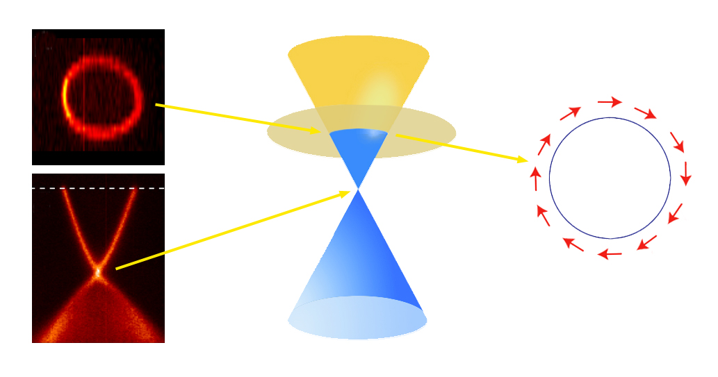
The band structure of the surface states of a topological insulator like Bi2Se3 appear as two cones that meet at a point, called the Dirac point. There’s no gap at all between the valence and conduction bands, only a smooth transition with increasing energy. This is similar to the band structure of the fascinating material graphene, a single sheet of carbon atoms, the thinnest possible surface. ARPES diagrams of band structures like these look like slices through the cones, an X centered on the Dirac point.
Although graphene and topological insulators have similar band structures, other electronic characteristics are very different. The combinations of different speeds and orientations equivalent to a material’s highest particle energies (at zero degrees) make up its momentum space, mapped by the Fermi surface. While the Fermi surface of graphene lies between the conical bands at the Dirac point, this is not true of TIs. The Fermi surface of Bi2Se3 cuts high across the conical conduction band, mapping a perfect circle. It’s as if the circular Fermi surface were drawn right on the surface of the topological insulator, showing how spin-locked surface electrons must change their spin orientation as they follow this continually curving path.
Values including electron-phonon coupling can be calculated from the diagrams that ARPES builds up. ARPES measures of Bi2Se3 show that coupling remains among the weakest ever reported for any material, even as the temperature approaches room temperature.

ARPES maps the electronic properties, including the band structure and Fermi surface, of the topological insulator bismuth selenide (left). Like graphene, the lower energy valence band of a topological insulator meets the higher energy conduction band at a point, the Dirac point, with no gap between the bands (center). Unlike graphene, however, the Fermi surface of a TI does not usually pass through the Dirac point. For surface electrons, distinct spin states (red arrows) are associated with each different orientation in momentum space (right).
Says Fedorov, “Although there’s still a long way to go, the experimental confirmation that electron-phonon coupling is very small underlines Bi2Se3’s practical potential.” With continued progress, the spin-locked electronic states of room-temperature topological insulators could open a gateway for spintronic devices – and for more exotic possibilities as well.
For example, by layering a superconducting material onto the surface of a topological insulator – a feat recently achieved by a group of Chinese scientists working at beamline 12.0.1 – it may be possible to create a theoretical but yet unseen particle that is its own antiparticle, one that could persist in the material undisturbed for long periods. Discovery of these so-called Majorana fermions would be an achievement in itself, and could also provide a way of overcoming the main obstacle to realizing a working quantum computer, a method of indefinitely storing data as “qubits.”
The experimental examination of strong, 3-D topological insulators is a field hardly more than five years old, and the potential rewards, both for fundamental and applied science, have only begun to be explored.
###
“Measurement of an exceptionally weak electron-phonon coupling on the surface of the topological insulator Bi2Se3 using angle-resolved photoemission spectroscopy,” by Z.-H. Pan, A. V. Fedorov, D. Gardner, Y. S. Lee, S. Chu, and T. Valla, appears in Physical Review Letters and is available online at prl.aps.org/abstract/PRL/v108/i18/e187001.
For the Brookhaven National Laboratory perspective on this research, visit www.bnl.gov/today/story.asp?ITEM_NO=3043.
A review of “Topological insulators,” by Charles Kane and Joel Moore, appears in Nature at www.physics.upenn.edu/~kane/pubs/p69.pdf.
Joel Moore’s historical article, “The birth of topological insulators,” appears in Nature at www.nature.com/nature/journal/v464/n7286/full/nature08916.html.
“The coexistence of superconductivity and topological order in the Bi2Se3 thin films,” by Y. L. Chen et al, appears in Science at www.sciencemag.org/content/336/6077/52.abstract.
The Advanced Light Source is a third-generation synchrotron light source producing light in the x-ray region of the spectrum that is a billion times brighter than the sun. A DOE national user facility, the ALS attracts scientists from around the world and supports its users in doing outstanding science in a safe environment. For more information visit www-als.lbl.gov/.
The U.S. Department of Energy’s Office of Science is the single largest supporter of basic research in the physical sciences in the United States, and is working to address some of the most pressing challenges of our time. For more information, please visit science.energy.gov.
Lawrence Berkeley National Laboratory addresses the world’s most urgent scientific challenges by advancing sustainable energy, protecting human health, creating new materials, and revealing the origin and fate of the universe. Founded in 1931, Berkeley Lab’s scientific expertise has been recognized with 13 Nobel prizes. The University of California manages Berkeley Lab for the U.S. Department of Energy’s Office of Science. For more, visit www.lbl.gov.