Over the years, computer chips have gotten smaller thanks to advances in materials science and manufacturing technologies. This march of progress, the doubling of transistors on a microprocessor roughly every two years, is called Moore’s Law. But there’s one component of the chip-making process in need of an overhaul if Moore’s law is to continue: the chemical mixture called photoresist. Similar to film used in photography, photoresist, also just called resist, is used to lay down the patterns of ever-shrinking lines and features on a chip.

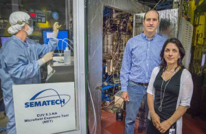
Paul Ashby and Deirdre Olynick of Berkeley Lab at the Advanced Light Source (ALS) Extreme Ultraviolet 12.0.1 Beamline. Credit: Roy Kaltschmidt, Berkeley Lab
Now, in a bid to continue decreasing transistor size while increasing computation and energy efficiency, chip-maker Intel has partnered with researchers from the U.S. Department of Energy’s Lawrence Berkeley National Lab (Berkeley Lab) to design an entirely new kind of resist. And importantly, they have done so by characterizing the chemistry of photoresist, crucial to further improve performance in a systematic way. The researchers believe their results could be easily incorporated by companies that make resist, and find their way into manufacturing lines as early as 2017.
The new resist effectively combines the material properties of two pre-existing kinds of resist, achieving the characteristics needed to make smaller features for microprocessors, which include better light sensitivity and mechanical stability, says Paul Ashby, staff scientist at Berkeley Lab’s Molecular Foundry, a DOE Office of Science user facility. “We discovered that mixing chemical groups, including cross linkers and a particular type of ester, could improve the resist’s performance.” The work is published this week in the journal Nanotechnology.
Finding a new kind of photoresist is “one of the largest challenges facing the semiconductor industry in the materials space,” says Patrick Naulleau, director of the Center for X-ray Optics (CXRO) at Berkeley Lab. Moreover, there’s been very little understanding of the fundamental science of how resist actually works at the chemical level, says Deirdre Olynick, staff scientist at the Molecular Foundry. “Resist is a very complex mixture of materials and it took so long to develop the technology that making huge leaps away from what’s already known has been seen as too risky,” she says. But now the lack of fundamental understanding could potentially put Moore’s Law in jeopardy, she adds.
To understand why resist is so important, consider a simplified explanation of how your microprocessors are made. A silicon wafer, about a foot in diameter, is cleaned and coated with a layer of photoresist. Next ultraviolet light is used to project an image of the desired circuit pattern including components such as wires and transistors on the wafer, chemically altering the resist.
Depending on the type of resist, light either makes it more or less soluble, so when the wafer is immersed in a solvent, the exposed or unexposed areas wash away. The resist protects the material that makes up transistors and wires from being etched away and can allow the material to be selectively deposited. This process of exposure, rinse and etch or deposition is repeated many times until all the components of a chip have been created.
The problem with today’s resist, however, is that it was originally developed for light sources that emit so-called deep ultraviolet light with wavelengths of 248 and 193 nanometers. But to gain finer features on chips, the industry intends to switch to a new light source with a shorter wavelength of just 13.5 nanometers. Called extreme ultraviolet (EUV), this light source has already found its way into manufacturing pilot lines. Unfortunately, today’s photoresist isn’t yet ready for high volume manufacturing.
“The semiconductor industry wants to go to smaller and smaller features,” explains Ashby. While extreme ultraviolet light is a promising technology, he adds, “you also need the resist materials that can pattern to the resolution that extreme ultraviolet can promise.” So teams led by Ashby and Olynick, which include Berkeley Lab postdoctoral researcher Prashant Kulshreshtha, investigated two types of resist. One is called crosslinking, composed of molecules that form bonds when exposed to ultraviolet light. This kind of resist has good mechanical stability and doesn’t distort during development—that is, tall, thin lines made with it don’t collapse. But if this is achieved with excessive crosslinking, it requires long, expensive exposures. The second kind of resist is highly sensitive, yet doesn’t have the mechanical stability.

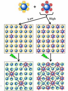
When a low concentrations of crosslinker is added to resist (left), it is able to pattern smaller features and doesn’t require longer, expensive exposures as with a high concentrations of crosslinker (right). Credit: Prashant Kulshreshtha, Berkeley Lab
When the researchers combined these two types of resist in various concentrations, they found they were able to retain the best properties of both. The materials were tested using the unique EUV patterning capabilities at the CXRO. Using the Nanofabrication and Imaging and Manipulation facilities at the Molecular Foundry to analyze the patterns, the researchers saw improvements in the smoothness of lines created by the photoresist, even as they shrunk the width. Through chemical analysis, they were also able to see how various concentrations of additives affected the cross-linking mechanism and resulting stability and sensitivity.
The researchers say future work includes further optimizing the resist’s chemical formula for the extremely small components required for tomorrow’s microprocessors. The semiconductor industry is currently locking down its manufacturing processes for chips at the so-called 10-nanometer node. If all goes well, these resist materials could play an important role in the process and help Moore’s Law persist. This research was funded by the Intel Corporation, JSR Micro, and the DOE Office of Science (Basic Energy Sciences).
###
Lawrence Berkeley National Laboratory addresses the world’s most urgent scientific challenges by advancing sustainable energy, protecting human health, creating new materials, and revealing the origin and fate of the universe. Founded in 1931, Berkeley Lab’s scientific expertise has been recognized with 13 Nobel prizes. The University of California manages Berkeley Lab for the U.S. Department of Energy’s Office of Science. For more, visit www.lbl.gov.
For over a decade Berkeley Lab’s Center for X-Ray Optics has conducted photolithography-related research, including world-leading programs in optics, masks, and materials — most conducted on three CXRO beamlines at the Advanced Light Source. For more information on CXRO, visit www.cxro.lbl.gov. For more information about the Advanced light source, visit www.als.lbl.gov.
The Molecular Foundry is one of five DOE Nanoscale Science Research Centers (NSRCs), national user facilities for interdisciplinary research at the nanoscale, supported by the DOE Office of Science. Together the NSRCs comprise a suite of complementary facilities that provide researchers with state-of-the-art capabilities to fabricate, process, characterize and model nanoscale materials, and constitute the largest infrastructure investment of the National Nanotechnology Initiative. The NSRCs are located at DOE’s Argonne, Brookhaven, Lawrence Berkeley, Oak Ridge and Sandia and Los Alamos National Laboratories. For more information about the DOE NSRCs, please visit http://science.energy.gov. For more information about the Molecular Foundry, visit http://foundry.lbl.gov/.
