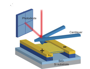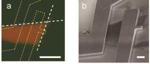
To measure in-plane piezoelectric stress, an MoS2 film was suspended on HSQ posts and clamped by two Au electrodes. When the film was indented with a scanning AFM probe, the induced stress changed the load on the cantilever, which was observed by the deflection of a laser beam.
A door has been opened to low-power off/on switches in micro-electro-mechanical systems (MEMS) and nanoelectronic devices, as well as ultrasensitive bio-sensors, with the first observation of piezoelectricity in a free standing two-dimensional semiconductor by a team of researchers with the U.S. Department of Energy (DOE)’s Lawrence Berkeley National Laboratory (Berkeley Lab).
Xiang Zhang, director of Berkeley Lab’s Materials Sciences Division and an international authority on nanoscale engineering, led a study in which piezoelectricity – the conversion of mechanical energy into electricity or vice versa – was demonstrated in a free standing single layer of molybdenum disulfide, a 2D semiconductor that is a potential successor to silicon for faster electronic devices in the future.
“Piezoelectricity is a well-known effect in bulk crystals, but this is the first quantitative measurement of the piezoelectric effect in a single layer of molecules that has intrinsic in-plane dipoles,” Zhang says. “The discovery of piezoelectricity at the molecular level not only is fundamentally interesting, but also could lead to tunable piezo-materials and devices for extremely small force generation and sensing.”

Xiang Zhang directs Berkeley Lab’s Materials Sciences Division (photo by Roy Kaltschmidt, Berkeley Lab)
Zhang, who holds the Ernest S. Kuh Endowed Chair at the University of California (UC) Berkeley and is a member of the Kavli Energy NanoSciences Institute at Berkeley, is the corresponding author of a paper in Nature Nanotechnology describing this research. The paper is titled “Observation of Piezoelectricity in Free-standing Monolayer MoS2.” The co-lead authors are Hanyu Zhu and Yuan Wang, both members of Zhang’s UC Berkeley research group. (See below for a complete list of co-authors.)
Since its discovery in 1880, the piezoelectric effect has found wide application in bulk materials, including actuators, sensors and energy harvesters. There is rising interest in using nanoscale piezoelectric materials to provide the lowest possible power consumption for on/off switches in MEMS and other types of electronic computing systems. However, when material thickness approaches a single molecular layer, the large surface energy can cause piezoelectric structures to be thermodynamically unstable.
Over the past couple of years, Zhang and his group have been carrying out detailed studies of molybdenum disulfide, a 2D semiconductor that features high electrical conductance comparable to that of graphene, but, unlike graphene, has natural energy band-gaps, which means its conductance can be switched off.
“Transition metal dichalcogenides such as molybdenum disulfide can retain their atomic structures down to the single layer limit without lattice reconstruction, even in ambient conditions,” Zhang says. “Recent calculations predicted the existence of piezoelectricity in these 2D crystals due to their broken inversion symmetry. To test this, we combined a laterally applied electric field with nano-indentation in an atomic force microscope for the measurement of piezoelectrically-generated membrane stress.”

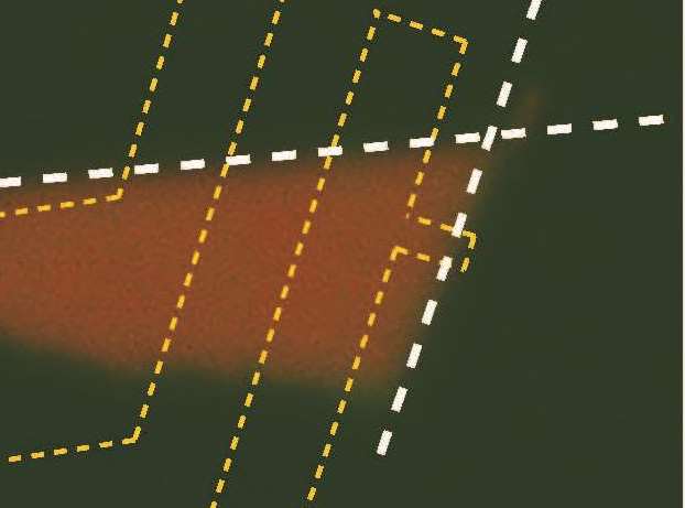
To maximize piezoelectric coupling, electrodes (yellow dashed lines) were defined parallel to the zigzag edges (white dashed lines) of the MoS2 monolayer. Green and red colors denote the intensity of reflection and photoluminescence respectively.
Zhang and his group used a free-standing molybdenum disulfide single layer crystal to avoid any substrate effects, such as doping and parasitic charge, in their measurements of the intrinsic piezoelectricity. They recorded a piezoelectric coefficient of 2.9×10⁻¹⁰ C/m, which is comparable to many widely used materials such as zinc oxide and aluminum nitride.
“Knowing the piezoelectric coefficient is important for designing atomically thin devices and estimating their performance,” says Nature paper co-lead author Zhu. “The piezoelectric coefficient we found in molybdenum disulfide is sufficient for use in low-power logic switches and biological sensors that are sensitive to molecular mass limits.”
Zhang, Zhu and their co-authors also discovered that if several single layers of molybdenum disulfide crystal were stacked on top of one another, piezoelectricity was only present in the odd number of layers (1,3,5, etc.)
“This discovery is interesting from a physics perspective since no other material has shown similar layer-number sensitivity,” Zhu says. “The phenomenon might also prove useful for applications in which we want devices consisting of as few as possible material types, where some areas of the device need to be non-piezoelectric.”
In addition to logic switches and biological sensors, piezoelectricity in molybdenum disulfide crystals might also find use in the potential new route to quantum computing and ultrafast data-processing called “valleytronics.” In valleytronics, information is encoded in the spin and momentum of an electron moving through a crystal lattice as a wave with energy peaks and valleys.
“Some types of valleytronic devices depend on absolute crystal orientation, and piezoelectric anisotropy can be employed to determine this,’ says Nature paper co-lead author Wang. “We are also investigating the possibility of using piezoelectricity to directly control valleytronic properties such as circular dichroism in molybdenum disulfide.”
In addition to Zhang, Zhu and Wang, other co-authors of the Nature paper were Jun Xiao, Ming Liu, Shaomin Xiong, Zi Jing Wong, Ziliang Ye, Yu Ye and Xiaobo Yin.
This research was supported by Light-Material Interactions in Energy Conversion, an Energy Frontier Research Center led by the California Institute of Technology, in which Berkeley Lab is a major partner. The Energy Frontier Research Center program is supported by DOE’s Office of Science.
Additional Information
For more about the research of Xiang Zhang go here
Xiang Zhang can be reached for comment at (Office) (510-643-0638) or (Mobile) (510-206-4792)
# # #
Lawrence Berkeley National Laboratory addresses the world’s most urgent scientific challenges by advancing sustainable energy, protecting human health, creating new materials, and revealing the origin and fate of the universe. Founded in 1931, Berkeley Lab’s scientific expertise has been recognized with 13 Nobel prizes. The University of California manages Berkeley Lab for the U.S. Department of Energy’s Office of Science. For more, visit www.lbl.gov.
The DOE Office of Science is the single largest supporter of basic research in the physical sciences in the United States and is working to address some of the most pressing challenges of our time. For more information, please visit science.energy.gov.
