
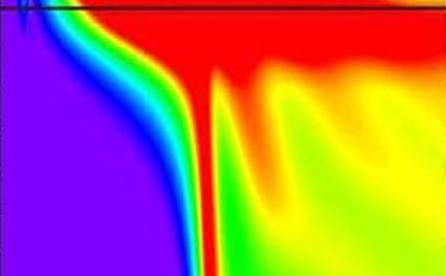
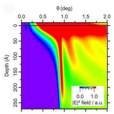
A new X-ray based technique for studying buried interfaces reveals that the more the incident angle increases, the deeper the X-rays penetrate the system, allowing for depth-resolved analysis of the system.
The nanoscale device community has shown great interest in exploiting the unique properties of ferroelectric materials for encoding information. But the circuitry for reading information stored in the polarization of these materials has prohibited its adaptation to extremely small scales. Now, researchers at Berkeley Lab and the Soleil Synchrotron in Paris have developed a new technique that provides key information for an alternative decoding method, where better understanding will help to fully harness the properties of these devices.
“By doing photoelectron spectroscopy in a near-total-reflection geometry, we can selectively change the depth of emission of the electrons, as well as create standing waves that sweep through the sample, thus providing a new tool for investigating buried interfaces,” says Chuck Fadley, a physicist at Berkeley Lab’s Materials Sciences Division, who led this work. “The basic idea for such near total reflection work goes back to our 1977 proof-of-concept study, but the method can now be fully exploited with modern synchrotron radiation sources and instrumentation.”
Manuel Bibes, of the CNR/Thales Laboratory in Paris, who synthesized the samples studied, says “The NTR method is an exciting new development because it provides quantitative information on the local charge density at the interface without the need for specific lithography or specimen preparation. NTR is thus a fast, efficient and versatile tool, ideal for systematic studies of interface-engineered samples such as those that we are interested in here at CNRS/Thales.”
Fadley, who also holds an appointment at the University of California Davis, is a group co-author of a paper describing this research in the journal Nano Letters. The paper is titled “Depth Profiling Charge Accumulation from a Ferroelectric into a Doped Mott Insulator.” The lead authors of the paper are Maya Marinova from the Laboratoire de Physique des Solides, Université Paris Sud, and Julien Rault of the Soleil Synchrotron, at the time of the measurements a French-supported postdoc in the Fadley group.
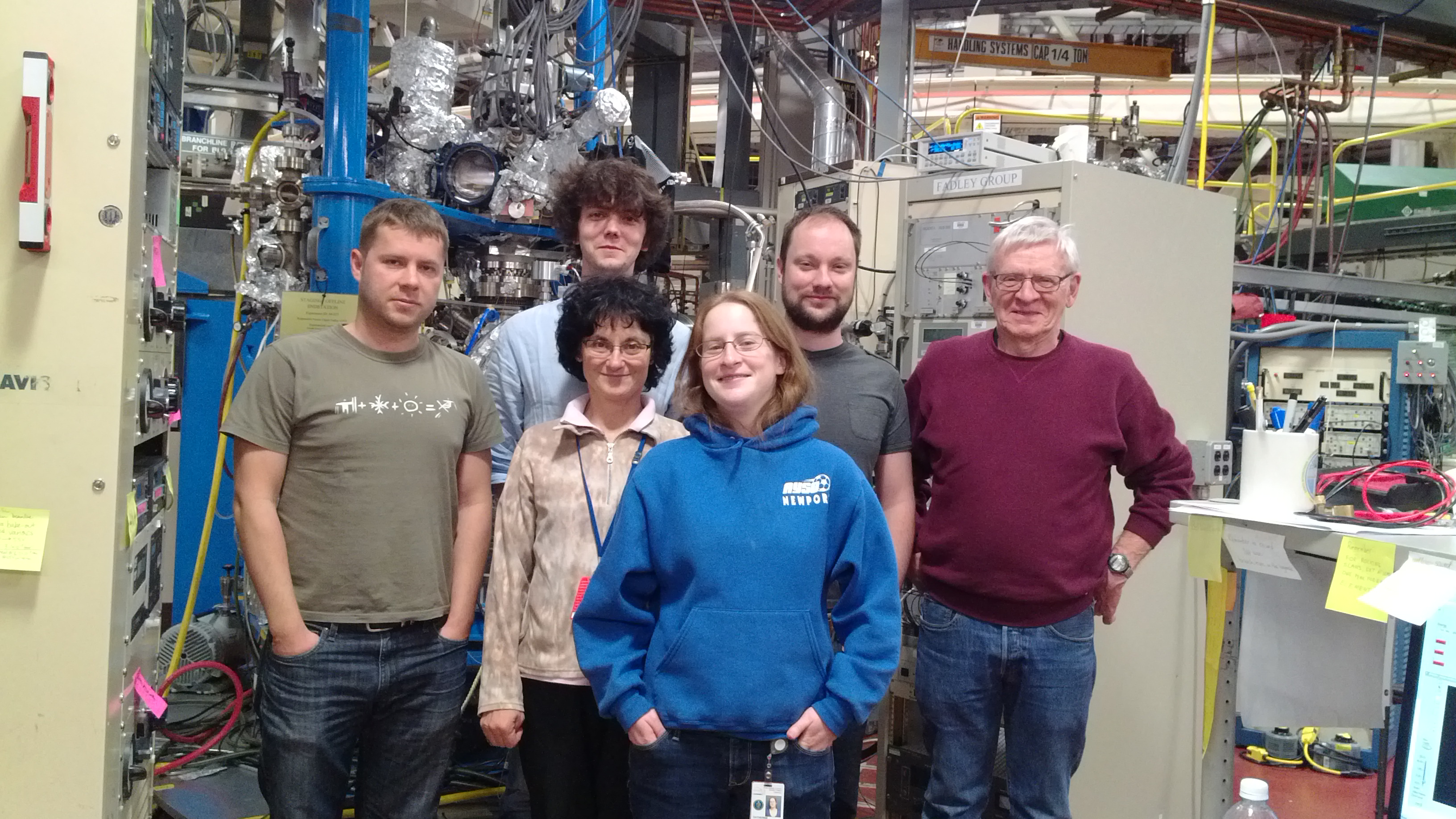
At ALS Beamline 9.3.1: Top row from left: Slavomir Nemsak, Julien Rault, Gunnar Palsson, Chuck Fadley; bottom row: Giuseppina Conti, Catherine Conlon.
Working at the Hard X-ray Photoemission Facility at Beamline 9.3.1 of Berkeley Lab’s Advanced Light Source, a DOE Office of Science User Facility, Fadley, Rault and their colleagues measured photoelectron peaks from different elements as the X-ray incidence angle was decreased until the total reflection condition at which no photoelectrons were emitted. Through various measurements and spectroscopic analyses, the team obtained a detailed depth profile of electric charge at the interface.
The sample interface, between ferroelectric BiFeO3 and a doped Mott insulator, shows promising behavior in its ability to switch from a less- to more-conducting state when exposed to an electric field. “A strong electroresistance effect is induced by the ferroelectric polarization of the BiFeO3 with a conductive electron gas being formed at the interface and in the Mott insulator,” explains Fadley. Such ferroelectric control opens the possibility of smaller or less energy-consuming switches or memory devices.
“Our colleagues in France supported these results by independent measurements using transmission electron microscopy and electron energy loss spectroscopy, thus confirming the general utility of the near-total-reflectivity photoemission method for studying many other types of interfaces with potential useful functionalities in technology,” Fadley concludes.
The research was funded in part by the DOE Office of Science.
Additional Information
For more about the research of Chuck Fadley go here
For more about the Advanced Light Source go here
For more about the Soleil Synchrotron go here