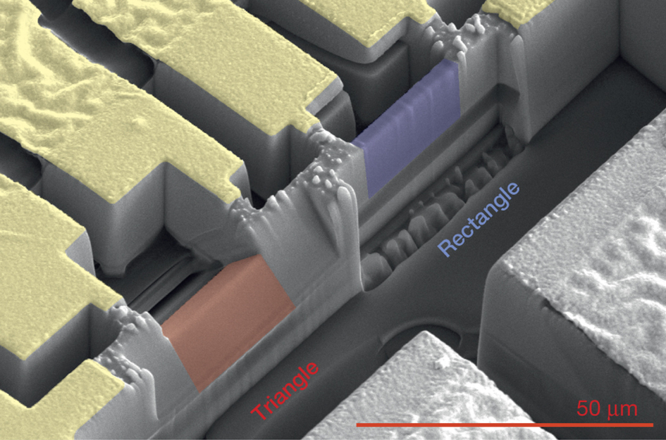
A scanning electron microscope image shows triangular (red) and rectangular (blue) samples of a semimetal crystal known as cadmium arsenide. The rectangular sample is about 0.8 microns (thousandths of a millimeter) thick, 3.2 microns tall and 5 microns long. The triangular sample has a base measuring about 2.7 microns. The design of the triangular samples, fabricated at Berkeley Lab’s Molecular Foundry, proved useful in mapping out the strange electron orbits exhibited by this material when exposed to a magnetic field. The red scale bar at lower right is 50 microns. (Credit: Nature, 10.1038/nature18276)
Researchers have created an exotic 3-D racetrack for electrons in ultrathin slices of a nanomaterial they fabricated at the Department of Energy’s Lawrence Berkeley National Laboratory (Berkeley Lab).
The international team of scientists from Berkeley Lab, UC Berkeley, and Germany observed, for the first time, a unique behavior in which electrons rotate around one surface, then through the bulk of the material to its opposite surface and back.
The possibility of developing so-called “topological matter” that can carry electrical current on its surface without loss at room temperature has attracted significant interest in the research community. The ultimate goal is to approach the lossless conduction of another class of materials, known as superconductors, but without the need for the extreme, freezing temperatures that superconductors require.
“Microchips lose so much energy through heat dissipation that it’s a limiting factor,” said James Analytis, a staff scientist at Berkeley Lab and assistant professor of physics at UC Berkeley who led the study, published in Nature. “The smaller they become, the more they heat up.”

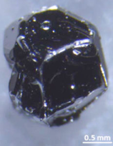
A single crystal of cadmium arsenide. Single crystals of this material, known as a “Dirac semimetal,” were cut to form nanoscale slices. The slices, when exposed to a magnetic field, exhibited an odd, roundabout electron path. The material could help scientists unlock the secrets of a class of materials that could be used in next-generation electronics. (Credit: Nature, 10.1038/nature18276)
The studied material, an inorganic semimetal called cadmium arsenide (Cd3As2), exhibits quantum properties—which are not explained by the classical laws of physics—that offer a new approach to reducing waste energy in microchips. In 2014, scientists discovered that cadmium arsenide shares some electronic properties with graphene, a single-atom-thick material also eyed for next-generation computer components, but in a 3-D form.
“What’s exciting about these phenomena is that, in theory, they are not affected by temperature, and the fact they exist in three dimensions possibly makes fabrication of new devices easier,” Analytis said.
The cadmium arsenide samples displayed a quantum property known as “chirality” that couples an electron’s fundamental property of spin to its momentum, essentially giving it left- or right-handed traits. The experiment provided a first step toward the goal of using chirality for transporting charge and energy through a material without loss.
In the experiment, researchers manufactured and studied how electric current travels in slices of a cadmium arsenic crystal just 150 nanometers thick, or about 600 times smaller than the width of a human hair, when subjected to a high magnetic field.
The crystal samples were crafted at Berkeley Lab’s Molecular Foundry, which has a focus in building and studying nanoscale materials, and their 3-D structure was detailed using X-rays at Berkeley Lab’s Advanced Light Source.
Many mysteries remain about the exotic properties of the studied material, and as a next step researchers are seeking other fabrication techniques to build a similar material with built-in magnetic properties, so no external magnetic field is required.
“This isn’t the right material for an application, but it tells us we’re on the right track,” Analytis said.
If researchers are successful in their modifications, such a material could conceivably be used for constructing interconnects between multiple computer chips, for example, for next-generation computers that rely on an electron’s spin to process data (known as “spintronics”), and for building thermoelectric devices that convert waste heat to electric current.
It wasn’t clear at first whether the research team would even be able to manufacture a pure enough sample at the tiny scale required to carry out the experiment, Analytis said.
“We wanted to measure the surface states of electrons in the material. But this 3-D material also conducts electricity in the bulk—it’s central region—as well as at the surface,” he said. As a result, when you measure the electric current, the signal is swamped by what is going on in the bulk so you never see the surface contribution.”
So they shrunk the sample from millionths of a meter to the nanoscale to give them more surface area and ensure that the surface signal would be the dominant one in an experiment.

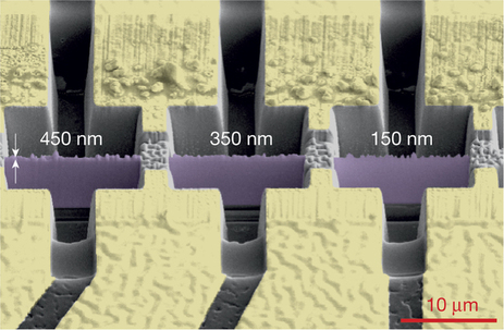
This image, produced by a scanning electron microscope, shows three sheets of a crystal material called cadmium arsenide. The finely polished rectangular sheets (purple) were sliced from the same crystal in varying thicknesses. They measure about 4 microns (thousandths of a millimeter) tall by 10 microns wide. (Credit: Nature, 10.1038/nature18276)
“We decided to do this by shaping samples into smaller structures using a focused beam of charged particles,” he said. “But this ion beam is known to be a rough way to treat the material—it is typically intrinsically damaging to surfaces, and we thought it was never going to work.”
But Philip J.W. Moll, now at the Max Planck Institute for Chemical Physics of Solids in Germany, found a way to minimize this damage and provide finely polished surfaces in the tiny slices using tools at the Molecular Foundry. “Cutting something and at the same time not damaging it are natural opposites. Our team had to push the ion beam fabrication to its limits of low energy and tight beam focus to make this possible.”
When researchers applied an electric current to the samples, they found that electrons race around in circles similar to how they orbit around an atom’s nucleus, but their path passes through both the surface and the bulk of the material.
The applied magnetic field pushes the electrons around the surface. When they reach the same energy and momentum of the bulk electrons, they get pulled by the chirality of the bulk and pushed through to the other surface, repeating this oddly twisting path until they are scattered by material defects.
The experiment represents a successful marriage of theoretical approaches with the right materials and techniques, Analytis said.
“This had been theorized by Andrew Potter on our team and his co-workers, and our experiment marks the first time it was observed,” Analytis said. “It is very unusual—there is no analogous phenomena in any other system. The two surfaces of the material ‘talk’ to each other over large distances due to their chiral nature.”
“We had predicted this behavior as a way to measure the unusual properties expected in these materials, and it was very exciting to see these ideas come to life in real experimental systems,” said Potter, an assistant physics professor at the University of Texas at Austin. “Philip and collaborators made some great innovations to produce extremely thin and high-quality samples, which really made these observations possible for the first time.”
Researchers also learned that disorder in the patterning of the material’s crystal surface doesn’t seem to affect the behavior of electrons there, though disorder in the central material does have an impact on whether the electrons move across the material from one surface to the other.
The motion of the electrons exhibits a dual handedness, with some electrons traveling around the material in one direction and others looping around in an opposite direction.
Researchers are now building on this work in designing new materials for ongoing studies, Analytis said. “We are using techniques normally restricted to the semiconductor industry to make prototype devices from quantum materials.”
Berkeley Lab’s Molecular Foundry and Advanced Light Source are both DOE Office of Science User Facilities.
This work was supported by the Department of Energy’s Office of Science, the Gordon and Betty Moore Foundation, and the Swiss Federal Institute of Technology in Zurich (ETH Zurich).
###
Lawrence Berkeley National Laboratory addresses the world’s most urgent scientific challenges by advancing sustainable energy, protecting human health, creating new materials, and revealing the origin and fate of the universe. Founded in 1931, Berkeley Lab’s scientific expertise has been recognized with 13 Nobel prizes. The University of California manages Berkeley Lab for the U.S. Department of Energy’s Office of Science. For more, visit www.lbl.gov.
DOE’s Office of Science is the single largest supporter of basic research in the physical sciences in the United States, and is working to address some of the most pressing challenges of our time. For more information, please visit science.energy.gov.
