
Next-generation solar cells made of super-thin films of semiconducting material hold promise because they’re relatively inexpensive and flexible enough to be applied just about anywhere.
Researchers are working to dramatically increase the efficiency at which thin-film solar cells convert sunlight to electricity. But it’s a tough challenge, partly because a solar cell’s subsurface realm—where much of the energy-conversion action happens—is inaccessible to real-time, nondestructive imaging. It’s difficult to improve processes you can’t see.
Now, scientists from the Department of Energy’s Lawrence Berkeley National Laboratory (Berkeley Lab) have developed a way to use optical microscopy to map thin-film solar cells in 3-D as they absorb photons.
The method, reported Nov. 15 in the journal Advanced Materials, was developed at the Molecular Foundry, a DOE Office of Science user facility located at Berkeley Lab. It images optoelectronic dynamics in materials at the micron scale, or much thinner than the diameter of a human hair. This is small enough to see individual grain boundaries, substrate interfaces, and other internal obstacles that can trap excited electrons and prevent them from reaching an electrode, which saps a solar cell’s efficiency.
So far, scientists have used the technique to better understand why adding a specific chemical to solar cells made of cadmium telluride (CdTe)—the most common thin-film material—improves the solar cells’ performance.

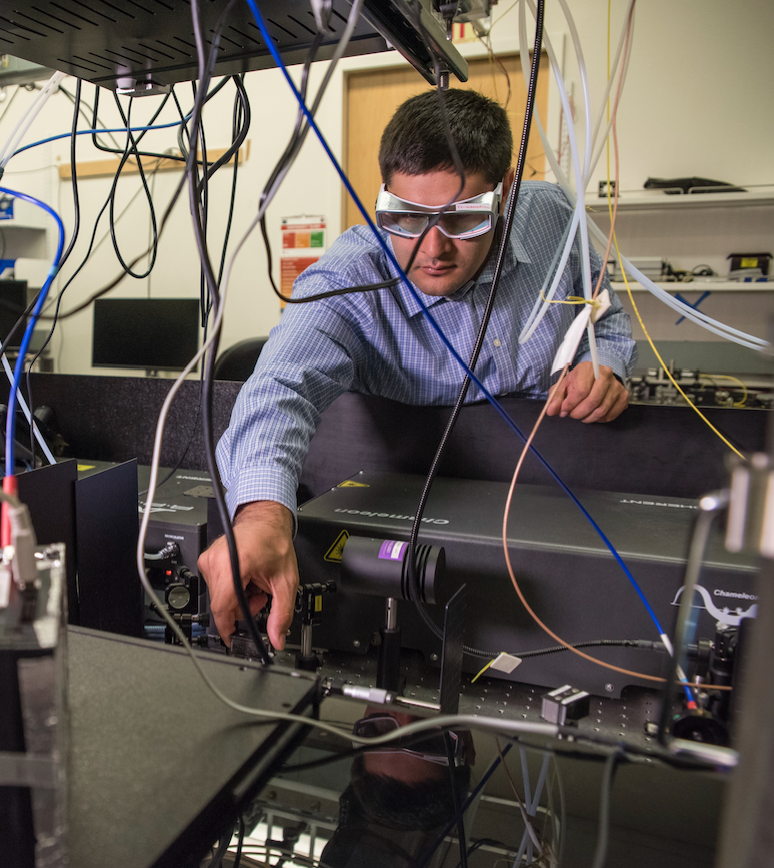
The Molecular Foundry’s Edward Barnard is part of a team of scientists that developed a new way to see inside solar cells. (Credit: Marilyn Chung)
“To make big gains in photovoltaic efficiency, we need to see what’s happening throughout a working photovoltaic material at the micron scale, both on the surface and below, and our new approach allows us to do that,” says Edward Barnard, a principal scientific engineering associate at the Molecular Foundry. He led the effort with James Schuck, the director of the Imaging and Manipulation of Nanostructures facility at the Molecular Foundry.
The imaging method is born out of a collaboration between Molecular Foundry scientists and Foundry users from PLANT PV Inc., an Alameda, California-based company. While fabricating new solar cell materials at the Molecular Foundry, the team found that standard optical techniques couldn’t image the inner-workings of the materials, so they developed the new technique to obtain this view. Next, scientists from the National Renewable Energy Laboratory came to the Molecular Foundry and used the new method to study CdTe solar cells.
To develop the approach, the scientists modified a technique called two-photon microscopy (which is used by biologists to see inside thick samples such as living tissue) so that it can be applied to bulk semiconductor materials.
The method uses a highly focused laser beam of infrared photons that penetrate inside the photovoltaic material. When two low-energy photons converge at the same pinpoint, there’s enough energy to excite electrons. These electrons can be tracked to see how long they last in their excited state, with long-lifetime electrons appearing as bright spots in microscopy images. In a solar cell, long-lifetime electrons are more likely to reach an electrode.
In addition, the laser beam can be systematically repositioned throughout a test-sized solar cell, creating a 3-D map of a solar cell’s entire optoelectronic dynamics.
The 3-D rendering on the left is a cadmium telluride solar cell without cadmium chloride treatment. The image on the right shows a solar cell that has been treated with cadmium chloride. It “lights up” much more uniformly throughout the material, both in the grains and the spaces in between. (Credit: Berkeley Lab)
The method has already shed light on the benefits of treating CdTe solar cells with cadmium chloride, which is often added during the fabrication process.
Scientists know cadmium chloride improves the efficiency of CdTe solar cells, but its effect on excited electrons at the micron scale is not well understood. Studies have shown that the chlorine ions tend to pile up at grain boundaries, but how this changes the lifetime of excited electrons is unclear.
Thanks to the new imaging technique, the researchers discovered the cadmium chloride treatment increases the lifetime of excited electrons at the grain boundaries, as well as within the grains themselves. This is easily seen in 3-D images of CdTe solar cells with and without the treatment. The treated solar cell “lights up” much more uniformly throughout the material, both in the grains and the spaces in between.
“Scientists have known that cadmium chloride passivation improves the lifetime of electrons in CdTe cells, but now we’ve mapped at the micron scale where this improvement occurs,” says Barnard.
The new imaging technique could help scientists make more informed decisions about improving a host of thin-film solar cell materials in addition to CdTe, such as perovskite and organic compounds.
“Researchers trying to push photovoltaic efficiency could use our technique to see if their strategies are working at the microscale, which will help them design better test-scale solar cells—and eventually full-sized solar cells for rooftops and other real-world applications,” he says.
The research was supported by the Department of Energy’s Office of Science and by a SunShot Initiative award from the Office of Energy Efficiency and Renewable Energy.
###
The U.S. Department of Energy SunShot Initiative is a collaborative national effort that aggressively drives innovation to make solar energy fully cost-competitive with traditional energy sources before the end of the decade. Through SunShot, the Energy Department supports efforts by private companies, universities, and national laboratories to drive down the cost of solar electricity to $0.06 per kilowatt-hour. Learn more at energy.gov/sunshot.
Lawrence Berkeley National Laboratory addresses the world’s most urgent scientific challenges by advancing sustainable energy, protecting human health, creating new materials, and revealing the origin and fate of the universe. Founded in 1931, Berkeley Lab’s scientific expertise has been recognized with 13 Nobel prizes. The University of California manages Berkeley Lab for the U.S. Department of Energy’s Office of Science. For more, visit www.lbl.gov.
DOE’s Office of Science is the single largest supporter of basic research in the physical sciences in the United States, and is working to address some of the most pressing challenges of our time. For more information, please visit science.energy.gov.
Additional information
- Go here for a photo and video montage of this research