

Illustration courtesy of Martin Hogborn/The Royal Swedish Academy of Sciences
Pioneering work by scientists at the Department of Energy’s Lawrence Berkeley National Laboratory (Berkeley Lab) played a key role in the 2017 Nobel Prize in chemistry, awarded today, honoring the development of cryo-electron microscopy, or cryo-EM, an imaging technique that has launched the fields of structural biology and biochemistry into an exciting new era of discovery.
Jacques Dubochet, Joachim Frank and Richard Henderson were awarded the Nobel for their foundational work in cryo-electron microscopy, which uses electrons to image samples that have been frozen mid-motion, expanding a technique that had previously been used for dead or inanimate matter to proteins and other biomolecules.
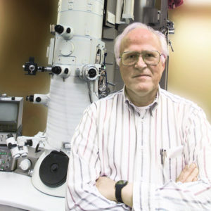
Robert Glaeser in front of his electron microscope equipped with a special cold stage. (Credit: Roy Kaltschmidt/Berkeley Lab)
In the scientific background detailing the development of cryo-EM, the Nobel committee highlighted a “series of critical developments” that has made it possible to take full advantage of the Nobel laureates’ achievements. They cited multiple papers co-authored by Berkeley Lab scientists Robert Glaeser, Ken Downing, Peter Denes, Howard Matis, Howard Weiman, and Fred Bieser.
Glaeser, who is also a UC Berkeley professor emeritus of biochemistry, was part of cryo-EM’s formative years. (Notably, Glaeser was an advisor for Nobel winner Joachim Frank when he was a postdoctoral researcher at UC Berkeley in the early 1970s. Frank was also a principal investigator at Berkeley Lab’s National Energy Research Scientific Computing Center, or NERSC, from 2004-2006.).
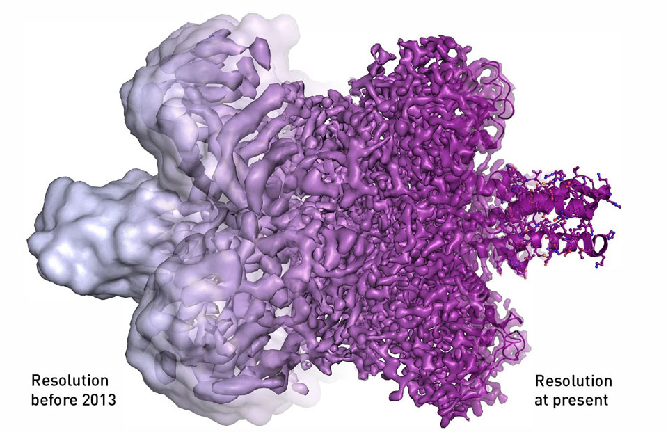
Glaeser and colleagues were among the first to show the importance of freezing samples to liquid nitrogen temperatures to protect them from the damage of intense electron beams. The Nobel committee noted Glaeser’s research on quantifying electron-induced radiation damage and providing guidance for the use of low-electron doses averaged over multiple samples.
To minimize damage to the sample, only a few electrons are used to image biological macromolecules, creating “noisy” images. The use of averaging is meant to deal with that “noise,” but it requires the samples to be precisely aligned. That created a serious bottleneck when managing tens to hundreds of thousands of images.
Enter the revolution enabled by new direct detector technology. In 2002, a UC San Diego professor approached Berkeley Lab’s Electronic Systems Group, then led by Denes, to pursue a new detector concept for electron microscopy that used crossed silicon strips. There had been a decades-long effort in the scientific community to improve the detector technology for electron microscopy, and Berkeley Lab was known to have expertise in detector R&D.
The particle physics and nuclear science communities were at the time eying another detector technology, known as CMOS APS, to track particles for their experiments, and Denes saw potential for that technology to be adapted for use in cryo-electron microscopy. CMOS APS detectors allowed for direct detection of electrons, which directly hit pixel sensors in a thin layer of silicon, providing direct “counting” of electrons and essentially eliminated the problem of noise.
After working on the concept, Denes connected with a group in the Lab’s Nuclear Science Division who were developing a detector technology for a particle collider experiment. Howard Matis, a retired Berkeley Lab physicist, recalled the successful effort – which also involved the Lab’s Howard Wieman and Fred Bieser – to develop the detector technology for proof-of-concept experiments and transfer the technology to UC San Diego for use in cryo-electron microscopy. Those experiments, in 2004 and 2005, were cited among other work in a scientific background document that accompanied the Nobel Prize announcement.
In later efforts, Denes led the development of the first large-scale CMOS APS detector for electron microscopy at the Transmission Electron Aberration-corrected Microscope (TEAM), a DOE-funded project at the National Center for Electron Microscopy (NCEM), based at Berkeley Lab’s Molecular Foundry.
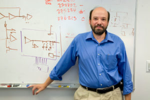
Peter Denes in front of a whiteboard at Berkeley Lab’s Advanced Light Source. (Credit: Roy Kaltschmidt/Berkeley Lab)
Denes pointed out that because the technology was initially designed for applications in materials science, it had to be fast to catch the movement of atoms and reveal how defects spread.
The Nobel committee specifically noted the advantage in speed as well as the improved signal-to-noise ratio and spatial resolution in this new generation of detectors.
A version of the Berkeley Lab camera has since been commercialized by Gatan, Inc., based in Pleasanton, California, and used in research labs, including that of Eva Nogales, faculty scientist at Berkeley Lab’s Molecular Biophysics and Integrated Bioimaging Division.
 Berkeley Lab’s work on improving electron microscopy technology is ongoing. Both Glaeser and Denes credited the collaborative ecosystem at Berkeley Lab for fostering innovation in electron microscopy.
This collaborative environment was highlighted at a recent workshop on the “Future of Electron Microscopy,” organized last year at Berkeley Lab by Denes; Andy Minor, NCEM director, and Paul Adams, director of the Molecular Biophysics and Integrated Bioimaging Division.
“I can’t think of any other place in the United States that has the combination of expertise and resources we have here in Berkeley,” said Denes. “The experience in electron microscopy, the strong background in biological and materials science research, the high-performance computing resources, the track record of developing innovative technology, are all here under one roof.”
In 2015, Denes, Downing and Uli Dahmen, former director of NCEM, were given Lab Lifetime Achievement Awards for their electron microscopy work at Berkeley Lab.
The Molecular Foundry and NERSC are both DOE Office of Science User Facilities.
RELATED INFO:
- The Development of Cryo-Electron Microscopy (Scientific Background on the Nobel Prize in Chemistry 2017)
- Workshop Focuses in on Electron Microscopy
- Cryo-EM’s Renaissance