
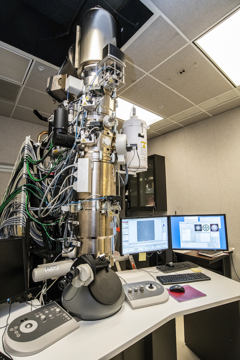
The high-stability, high-resolution Thermo Fisher “ThemIS” transmission electron microscope. (Credit: Marilyn Chung/Berkeley Lab)
By Laurie Chong
Researchers at the Department of Energy’s Lawrence Berkeley National Laboratory (Berkeley Lab) now have access to a unique new microscope that combines atomic-scale imaging capabilities with the ability to observe real-world sample properties and behavior in real time.
Housed at Berkeley Lab’s Molecular Foundry in partnership with the Materials Sciences Division, the new instrument is a high-stability, high-resolution Thermo Fisher “ThemIS” transmission electron microscope (TEM). The “IS” in its name emphasizes that it has been customized for in situ experiments, enabling researchers to study materials and reactions under natural conditions.
The ThemIS microscope will provide unprecedented insight into fundamental atomic-scale materials transformations that occur at solid-liquid interfaces, which is essential for making advances in battery and desalination technologies, for example.
Haimei Zheng, a staff scientist in Berkeley Lab’s Materials Sciences Division whose research group focuses on understanding, engineering, and controlling materials at solid-liquid interfaces – with a particular emphasis on sustainable energy, clean water, and the environment – was instrumental in acquiring the new microscope.
“In situ transmission electron microscopy enables direct observation of reactions and atomic pathways, provides key information on the structural dynamics of a material during transformations, and has the ability to correlate a material’s structure and properties,” she said, “but it has ultimately been limited by the speed and resolution of the microscope.”
She added, “With this advanced TEM and newly developed technologies, we are now able to image chemical reactions and study materials dynamics in liquids with a resolution that was previously impossible.”
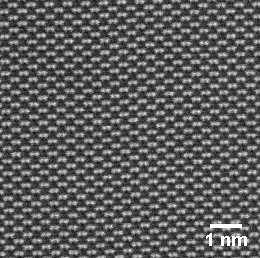
A silicon sample is seen at nanoscale resolution in this first image produced by the ThemIS transmission electron microscope (scale bar is 1 nanometer). (Credit: Molecular Foundry/Berkeley Lab)
Electron microscopes have expanded scientists’ ability to understand the world by making visible what was once invisible. A TEM uses electromagnetic lenses to focus electrons. Its focused beam of electrons passes through a sample and is scattered into either an image or a diffraction pattern. Since the necessarily thin samples (measuring from 10 to hundreds of nanometers, or billionths of a meter) are subjected to the high-vacuum environment inside the TEM, observations of materials in their relevant environment are challenging.
In order to overcome this challenge, in situ TEMs utilize special sample holders that allow a researcher to observe the physical behavior of materials in response to external stimuli such as temperature, environment, stress, and applied fields.
By studying samples in liquids or gases using these special holders, researchers can observe the atomic-scale details of nanoparticles and how they undergo changes in their reactive environments. This capability not only provides for a deeper understanding of chemical reactions, but it also allows for the study of a wider variety of nanoparticle systems where reaction pathways are still unknown.
“The microscope will provide researchers with new tools that expand the existing imaging and chemical analysis capabilities of our TitanX microscope, which has long been in high demand,” said Andy Minor, the facility director of the Foundry’s National Center for Electron Microscopy (NCEM). The TitanX is a predecessor high-resolution TEM.
The ThemIS microscope is the product of a joint effort between Berkeley Lab’s Materials Sciences Division and the Molecular Foundry, and is supported by the Department of Energy’s Office of Basic Energy Sciences.
The microscope’s customization includes the following features that make it optimal for in situ experiments:
- An image corrector for high-resolution TEM imaging.
- A “Ceta” camera for imaging a wide field of view at high resolution and relatively high speed (4,096-by-4,096-pixel resolution at 40 frames per second).
- A specialized “fast gun valve” that protects the microscope from gases that may be released during environmental in situ experiments.
- A “super-X quad-EDS detector” for elemental analysis, expanding NCEM’s high-resolution analytical capabilities.
The Molecular Foundry is a DOE Office of Science User Facility.
More info:
- If you’re a researcher who wants to use the ThemIS, visit the Foundry’s user program website and check out these technical specs. Questions? Contact Karen Bustillo.
- ThemIS overview
- About the National Center for Electron Microscopy at the Molecular Foundry
###
Lawrence Berkeley National Laboratory addresses the world’s most urgent scientific challenges by advancing sustainable energy, protecting human health, creating new materials, and revealing the origin and fate of the universe. Founded in 1931, Berkeley Lab’s scientific expertise has been recognized with 13 Nobel Prizes. The University of California manages Berkeley Lab for the U.S. Department of Energy’s Office of Science. For more, visit www.lbl.gov.
DOE’s Office of Science is the single largest supporter of basic research in the physical sciences in the United States, and is working to address some of the most pressing challenges of our time. For more information, please visit science.energy.gov.