
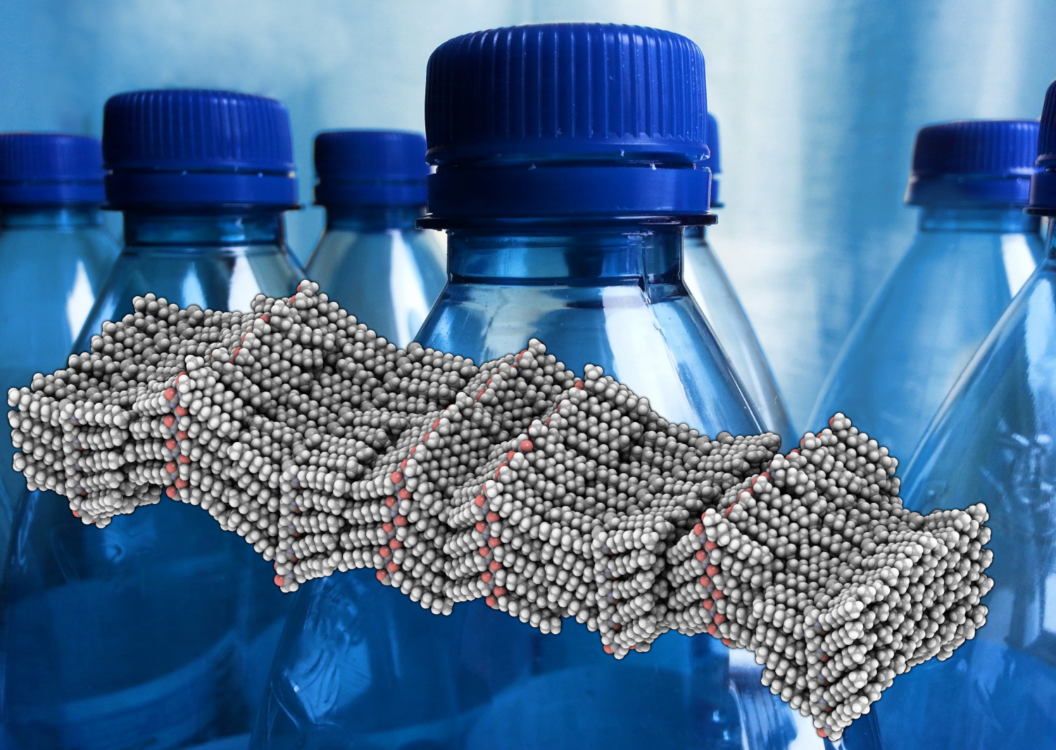
This image shows a rendering (gray and pink) of the molecular structure of a peptoid polymer that was studied by a team led by Berkeley Lab and UC Berkeley. The successful imaging of a polymer’s atomic-scale structure could inform new designs for plastics, like those that form the water bottles shown in the background. (Credit: Berkeley Lab, Charles Rondeau/PublicDomainPictures.net)
From water bottles and food containers to toys and tubing, many modern materials are made of plastics. And while we produce about 110 million tons per year of synthetic polymers like polyethylene and polypropylene worldwide for these plastic products, there are still mysteries about polymers at the atomic scale.
Because of the difficulty in capturing images of these materials at tiny scales, images of individual atoms in polymers have only been realized in computer simulations and illustrations, for example.
Now, a research team led by Nitash Balsara, a senior faculty scientist in the Materials Sciences Division at the Department of Energy’s Lawrence Berkeley National Laboratory (Berkeley Lab) and professor of chemical and biomolecular engineering at UC Berkeley, has adapted a powerful electron-based imaging technique to obtain an image of atomic-scale structure in a synthetic polymer. The team included researchers from Berkeley Lab and UC Berkeley.
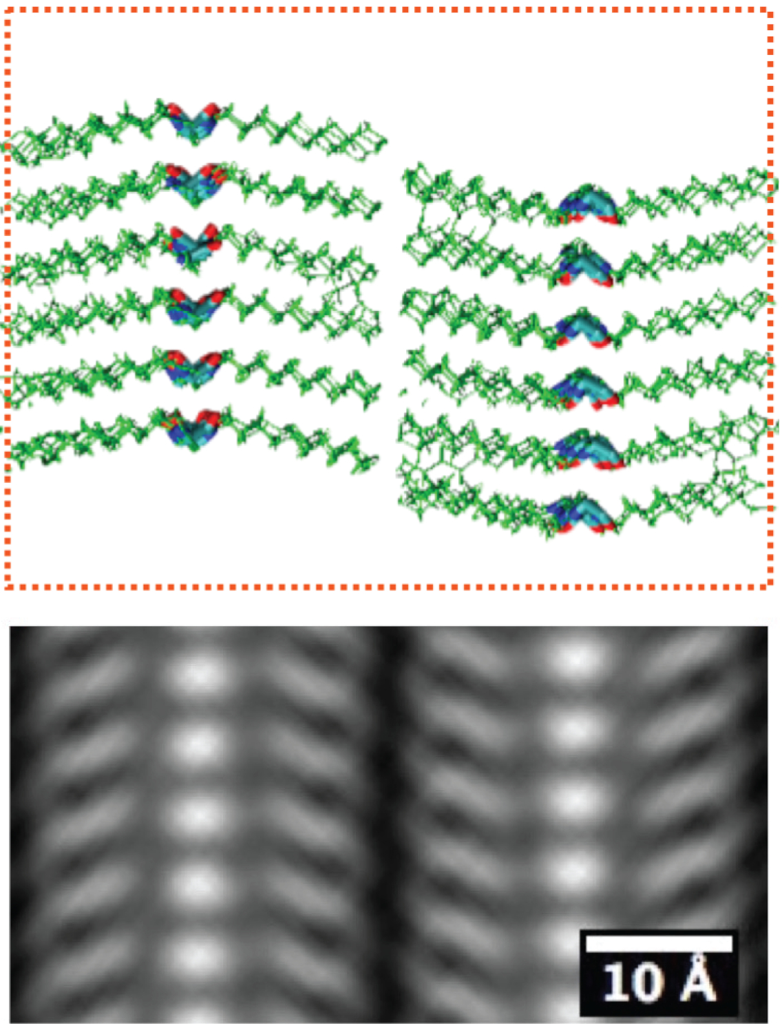
The simulated atomic-scale structure (top) and the averaged atomic-scale imaging (bottom) of a peptoid polymer sample. The sale bar is 10 angstroms, or 1 billionth of a meter. (Credit: Berkeley Lab, UC Berkeley)
The research could ultimately inform polymer fabrication methods and lead to new designs for materials and devices that incorporate polymers.
In their study, published in the American Chemical Society’s Macromolecules journal, the researchers detail the development of a cryogenic electron microscopy imaging technique, aided by computerized simulations and sorting techniques, that identified 35 arrangements of crystal structures in a peptoid polymer sample. Peptoids are synthetically produced molecules that mimic biological molecules, including chains of amino acids known as peptides.
The sample was robotically synthesized at Berkeley Lab’s Molecular Foundry, a DOE Office of Science User Facility for nanoscience research. Researchers formed sheets of crystallized polymers measuring about 5 nanometers (billionths of a meter) in thickness when dispersed in water.
“We conducted our experiments on the most perfect polymer molecules we could make,” Balsara said – the peptoid samples in the study were extremely pure compared to typical synthetic polymers.
The research team created tiny flakes of peptoid nanosheets, froze them to preserve their structure, and then imaged them using an electron beam. An inherent challenge in imaging materials with a soft structure, such as polymers, is that the beam used to capture images also damages the samples.
The direct cryogenic electron microscopy images, obtained using very few electrons to minimize beam damage, are too blurry to reveal individual atoms. Researchers achieved resolution of about 2 angstroms, which is two-tenths of nanometer (billionth of a meter), or about double the diameter of a hydrogen atom.
They achieved this by taking over 500,000 blurry images, sorting different motifs into different “bins,” and averaging the images in each bin. The sorting methods they used were based on algorithms developed by the structural biology community to image the atomic structure of proteins.
“We took advantage of technology that the protein-imaging folks had developed and extended it to human-made, soft materials,” Balsara said. “Only when we sorted them and averaged them did that blurriness become clear.”
Before these high-resolution images, Balsara said, the arrangement and variation of the different types of crystal structures was unknown.
“We knew that there were many motifs, but they are all different from each other in ways we didn’t know,” he said. “In fact, even the dominant motif in the peptoid sheet was a surprise.”

Researchers developed a colorized map (right) to show the distribution of different types of crystal structures (left) that they found in the polymer peptoid sample. The scale bar in the map image is 50 nanometers, or 50 billionths of a meter. (Credit: Berkeley Lab, UC Berkeley)
Balsara credited Ken Downing, a senior scientist in Berkeley Lab’s Molecular Biophysics and Integrated Bioimaging Division who passed away in August, and Xi Jiang, a project scientist in the Materials Sciences Division, for capturing the high-quality images that were central to the study and for developing the algorithms necessary to achieve atomic resolution in the polymer imaging.
Their expertise in cryogenic electron microscopy was complemented by Ron Zuckermann’s ability to synthesize model peptoids, David Prendergast’s knowledge of molecular dynamics simulations needed to interpret the images, Andrew Minor’s expertise in imaging metals at the atomic scale, and Balsara’s experience in the field of polymer science.
At the Molecular Foundry, Zuckermann directs the Biological Nanostructures facility, Prendergast directs the Theory facility, and Minor directs the National Center for Electron Microscopy and is also a professor of materials science and engineering at UC Berkeley. Much of the cryo-electron imaging was carried out at UC Berkeley’s Krios microscopy facility.
Balsara said that his own research into using polymers for batteries and other electrochemical devices could benefit from the research, as seeing the position of polymer atoms could greatly aid in the design of materials for these devices.
Atomic-scale images of polymers used in everyday life may need more sophisticated, automated filtering mechanisms that rely on machine learning, for example.
“We should be able to determine the atomic-scale structure of a wide variety of synthetic polymers such as commercial polyethylene and polypropylene, leveraging rapid developments in areas such as artificial intelligence, using this approach,” Balsara said.
Determining crystal structures can provide vital information for other applications, such as the development of drugs, as different crystal motifs could produce quite different binding properties and therapeutic effects, for example.
The work was conducted within the Soft Matter Electron Microscopy Program at Berkeley Lab, which is supported by the U.S. Department of Energy’s Office of Science; and by the Bay Area Cryo-EM Consortium.
###
Lawrence Berkeley National Laboratory addresses the world’s most urgent scientific challenges by advancing sustainable energy, protecting human health, creating new materials, and revealing the origin and fate of the universe. Founded in 1931, Berkeley Lab’s scientific expertise has been recognized with 13 Nobel Prizes. The University of California manages Berkeley Lab for the U.S. Department of Energy’s Office of Science. For more, visit www.lbl.gov.
DOE’s Office of Science is the single largest supporter of basic research in the physical sciences in the United States, and is working to address some of the most pressing challenges of our time. For more information, please visit the Office of Science website at http://science.energy.gov.