
This video provides an overview of the R&D effort to upgrade an electron microscope at Berkeley Lab’s Molecular Foundry with a superfast detector, the 4D Camera. The detector, which is linked to a supercomputer at Berkeley Lab via a high-speed data connection, can capture more images at a faster rate, revealing atomic-scale details across much larger areas than was possible before. (Credit: Marilyn Chung/Berkeley Lab)
Advances in electron microscopy – using electrons as imaging tools to see things well beyond the reach of conventional microscopes that use light – have opened up a new window into the nanoscale world and brought a wide range of samples into focus as never before.
Electron microscopy experiments can only use a fraction of the possible information generated as the microscope’s electron beam interacts with samples. Now, a team at the Department of Energy’s Lawrence Berkeley National Laboratory (Berkeley Lab) has designed a new kind of electron detector that captures all of the information in these interactions.
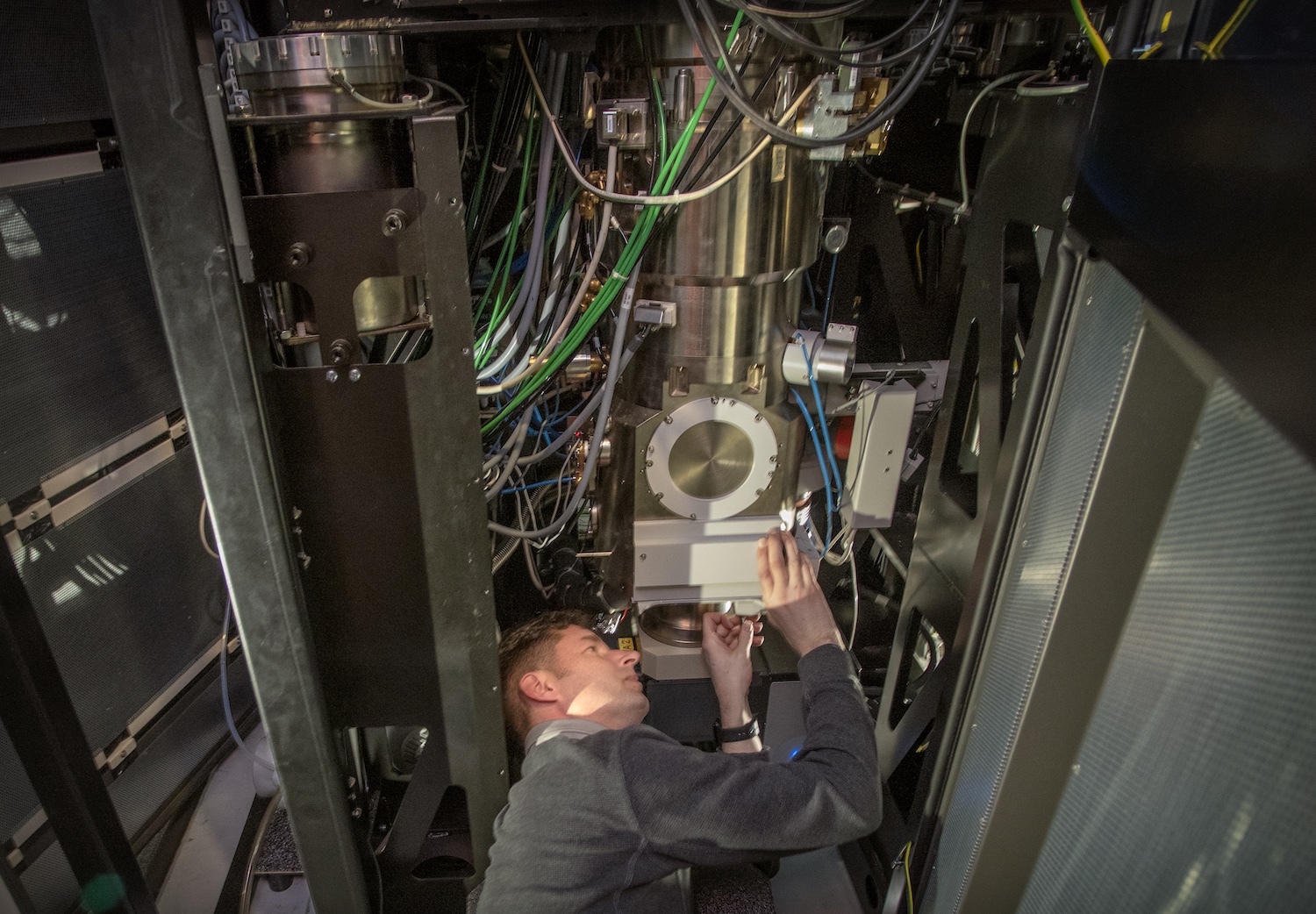
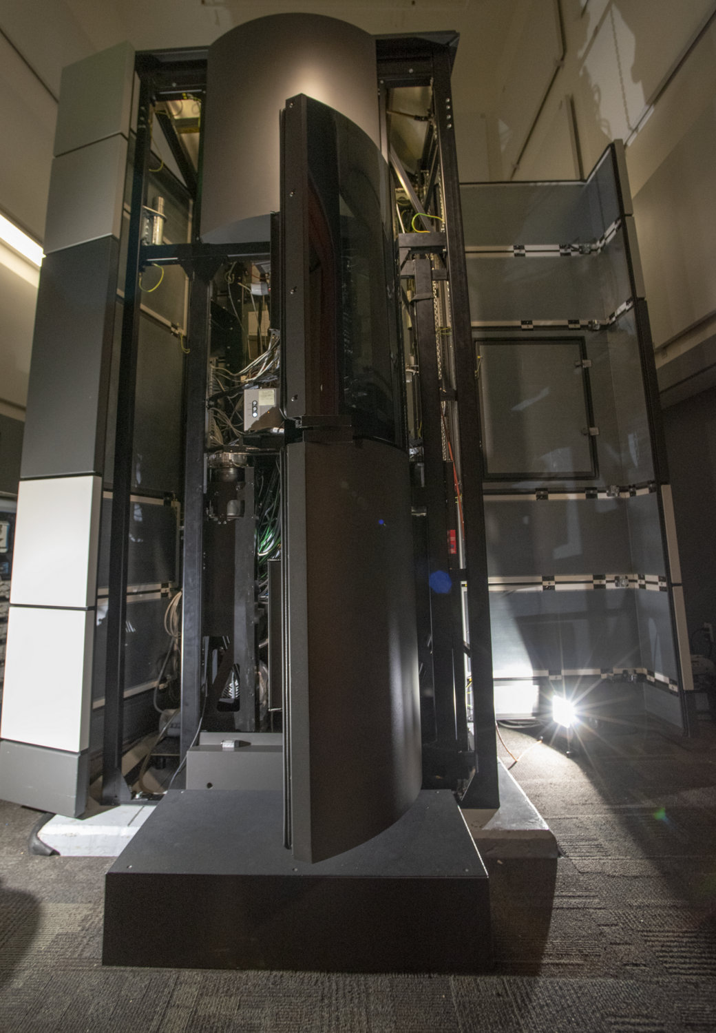
This new tool, a superfast detector installed Feb. 12 at Berkeley Lab’s Molecular Foundry, a nanoscale science user facility, captures more images at a faster rate, revealing atomic-scale details across much larger areas than was possible before. The Molecular Foundry and its world-class electron microscopes in the National Center for Electron Microscopy (NCEM) provide access to researchers from around the world.
The Transmission Electron Aberration-corrected Microscope (TEAM 0.5) at Berkeley Lab has been upgraded with a new detector that can capture atomic-scale images in millionths-of-a-second increments. (Credit: Thor Swift/Berkeley Lab)
Faster imaging can also reveal important changes that samples are undergoing and provide movies vs. isolated snapshots. It could, for example, help scientists to better explore working battery and microchip components at the atomic scale before the onset of damage.
The detector, which has a special direct connection to the Cori supercomputer at the Lab’s National Energy Research Scientific Computing Center (NERSC), will enable scientists to record atomic-scale images with timing measured in microseconds, or millionths of a second – 60 times faster than possible with existing detectors.
“It is the fastest electron detector ever made,” said Andrew Minor, NCEM facility director at the Molecular Foundry.
“It opens up a new time regime to explore with high-resolution microscopy. No one has ever taken continuous movies at this time resolution” using electron imaging, he said. “What happens there? There are all kinds of dynamics that might happen. We just don’t know because we’ve never been able to look at them before.” The new movies could reveal tiny deformations and movements in materials, for example, and show chemistry in action.
The development of the new detector, known as the “4D Camera” (for Dynamic Diffraction Direct Detector), is the latest in a string of pioneering innovations in electron microscopy, atomic-scale imaging, and high-speed data transfer and computing at Berkeley Lab that span several decades.
“Our group has been working for some time on making better detectors for microscopy,” said Peter Denes, a Berkeley Lab senior scientist and a longtime pioneer in the development of electron microscopy tools.
“You get a whole scattering pattern instead of just one point, and you can go back and reanalyze the data to find things that maybe you weren’t focusing on before,” Denes said. This quickly produces a complete image of a sample by scanning across it with an electron beam and capturing information based on the electrons that scatter off the sample.
Mary Scott, a faculty scientist at the Molecular Foundry, said that the unique geometry of the new detector allows studies of both light and heavyweight elements in materials side by side. “The reason you might want to perform one of these more complicated experiments would be to measure the positions of light elements, particularly in materials that might be really sensitive to the electron beam – like lithium in a battery material – and ideally you would be able to also precisely measure the positions of heavy elements in that same material,” she said.
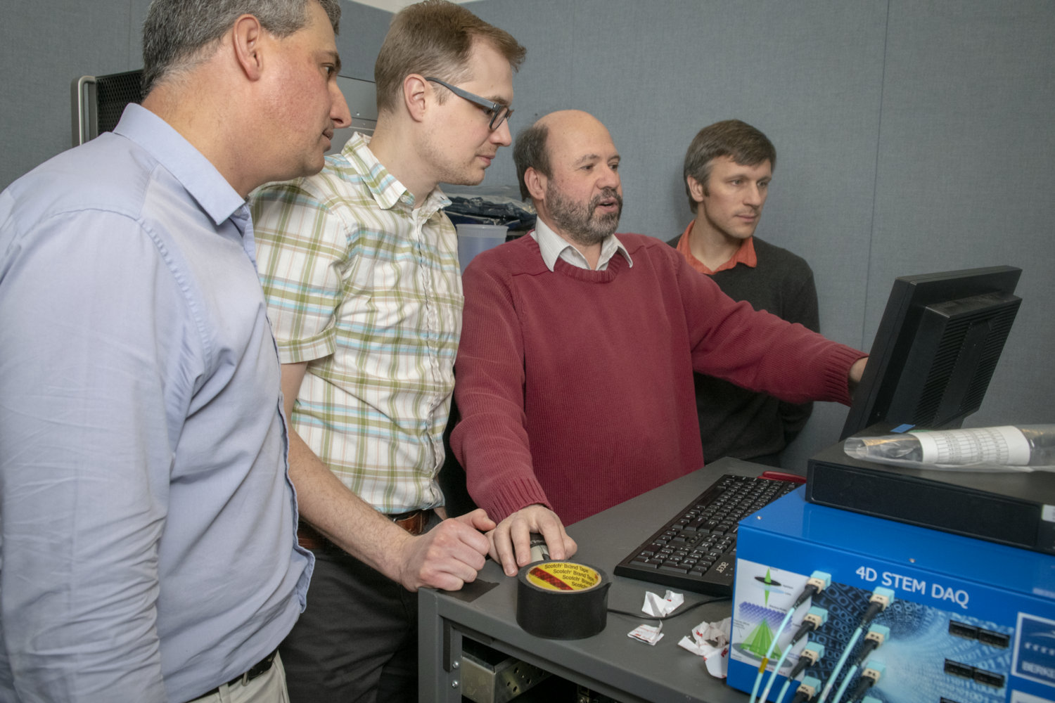
From left to right: Berkeley Lab’s Ian Johnson, Jim Ciston, Peter Denes, and Peter Ercius work on troubleshooting for a new, superfast detector, the 4D Camera, installed at the TEAM 0.5 microscope at Berkeley Lab’s Molecular Foundry. (Credit: Thor Swift/Berkeley Lab)
The new detector has been installed on the Transmission Electron Aberration-corrected Microscope 0.5 (TEAM 0.5) at the Molecular Foundry, which set high-resolution records when it launched at NCEM a decade ago and allows visiting researchers to access single-atom resolution for some samples. The detector will generate a whopping 4 terabytes of data per minute.
“The amount of data is equivalent to watching about 60,000 HD movies simultaneously,” said Peter Ercius, a staff scientist at the Molecular Foundry who specializes in 3D atomic-scale imaging.
Brent Draney, a networking architect at Berkeley Lab’s NERSC, said that Ercius and Denes had approached NERSC to see what it would take to build a system that could handle this huge, 400-gigabit stream of data produced by the 4D Camera.
His response: “We actually already have a system capable of doing that. What we really needed to do is to build a network between the microscope and the supercomputer.”
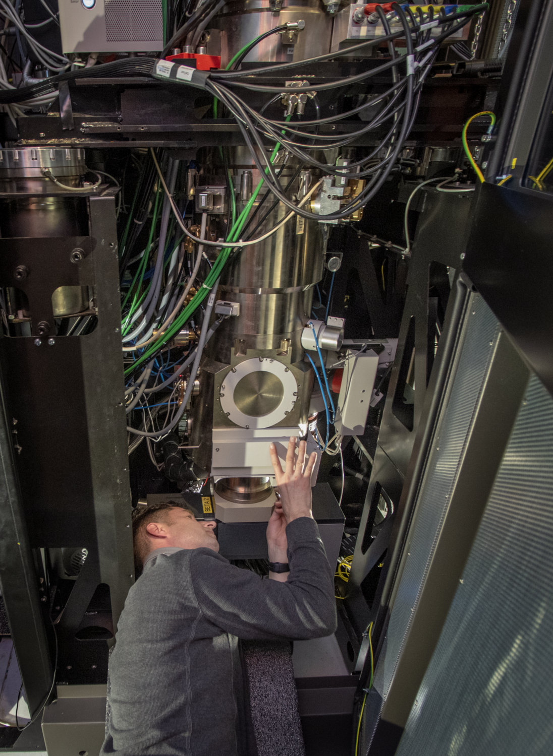
A technician works on the TEAM 0.5 microscope. The microscope has been upgraded with a superfast detector called the 4D Camera that can capture atomic-scale images in millionths-of-a-second increments. (Credit: Thor Swift/Berkeley Lab)
Camera data is transferred over about 100 fiber-optic connections into a high-speed ethernet connection that is about 1,000 times faster than the average home network, said Ian Johnson, a staff scientist in Berkeley Lab’s Engineering Division. The network connects the Foundry to the Cori supercomputer at NERSC.
Berkeley Lab’s Energy Sciences Network (ESnet), which connects research centers with high-speed data networks, participated in the effort.
Ercius said, “The supercomputer will analyze the data in about 20 seconds in order to provide rapid feedback to the scientists at the microscope to tell if the experiment was successful or not.”
Jim Ciston, another Molecular Foundry staff scientist, said, “We’ll actually capture every electron that comes through the sample as it’s scattered. Through this really large data set we’ll be able to perform ‘virtual’ experiments on the sample – we won’t have to go back and take new data from different imaging conditions.”
The work on the new detector and its supporting data systems should benefit other facilities that produce high volumes of data, such as the Advanced Light Source and its planned upgrade, and the LCLS-II project at SLAC National Accelerator Laboratory, Ciston noted.
The Advanced Light Source, ESnet, Molecular Foundry, and NERSC are DOE Office of Science User Facilities.
The development of the 4D Camera was supported by the Accelerator and Detector Research Program of the Department of Energy’s Office of Basic Energy Sciences, and work at the Molecular Foundry was supported by the DOE’s Office of Basic Energy Sciences.
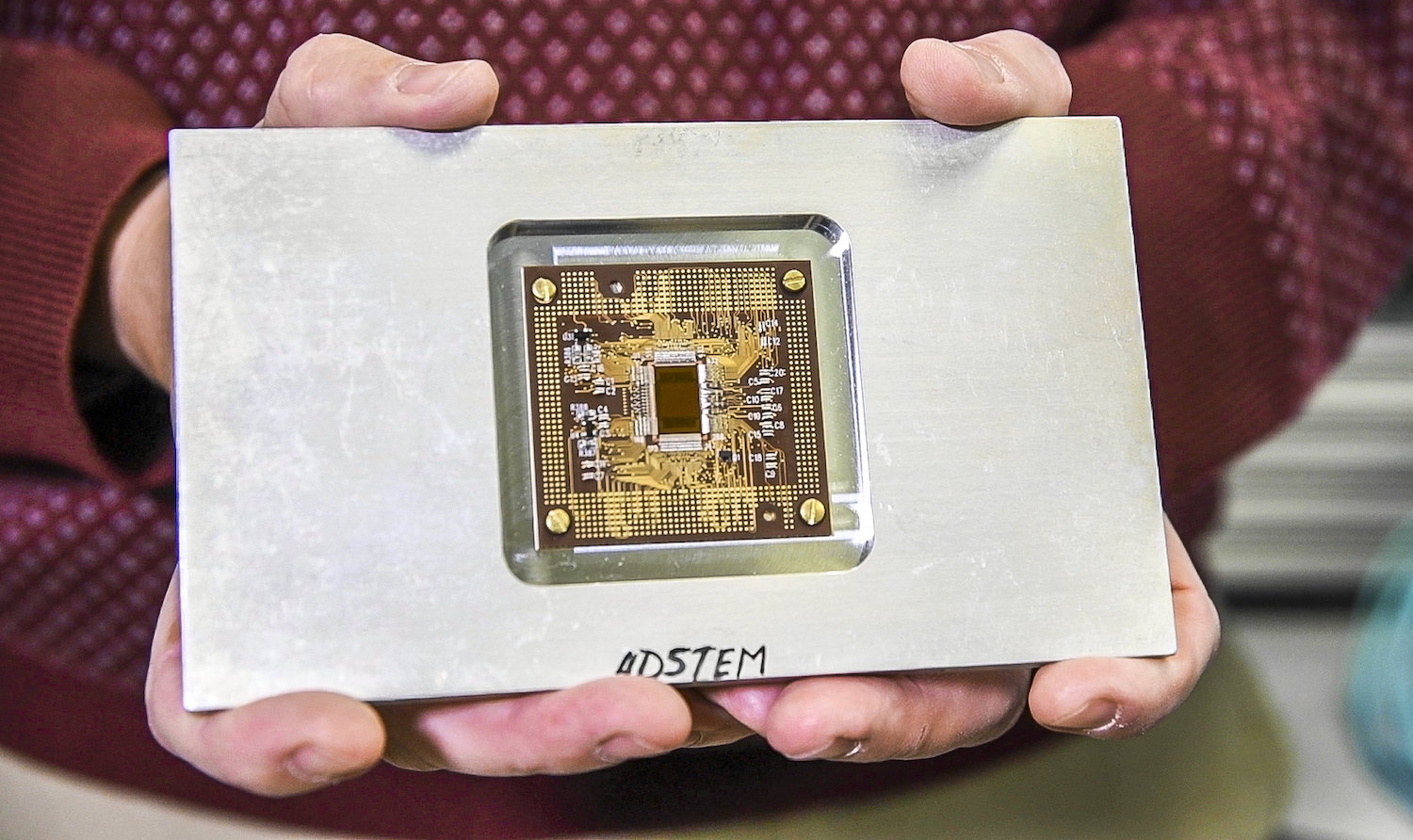
This computer chip is a component in a superfast detector called the 4D Camera. The detector is an upgrade for a powerful electron microscope at Berkeley Lab’s Molecular Foundry. (Credit: Marilyn Chung/Berkeley Lab)
###
Founded in 1931 on the belief that the biggest scientific challenges are best addressed by teams, Lawrence Berkeley National Laboratory and its scientists have been recognized with 13 Nobel Prizes. Today, Berkeley Lab researchers develop sustainable energy and environmental solutions, create useful new materials, advance the frontiers of computing, and probe the mysteries of life, matter, and the universe. Scientists from around the world rely on the Lab’s facilities for their own discovery science. Berkeley Lab is a multiprogram national laboratory, managed by the University of California for the U.S. Department of Energy’s Office of Science.
DOE’s Office of Science is the single largest supporter of basic research in the physical sciences in the United States, and is working to address some of the most pressing challenges of our time. For more information, please visit science.energy.gov.