
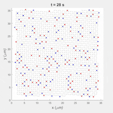
Magnetic monopoles in motion at 210 K. Red dots represent positive magnetic charges (north poles), while blue dots represent negative magnetic charges (south poles). (Credit: Farhan/Berkeley Lab)
A research team led by the Department of Energy’s Lawrence Berkeley National Laboratory (Berkeley Lab) has created a nanoscale “playground” on a chip that simulates the formation of exotic magnetic particles called monopoles. The study – published recently in Science Advances – could unlock the secrets to ever-smaller, more powerful memory devices, microelectronics, and next-generation hard drives that employ the power of magnetic spin to store data.
Follow the ‘ice rules’
For years, other researchers have been trying to create a real-world model of a magnetic monopole – a theoretical magnetic, subatomic particle that has a single north or south pole. These elusive particles can be simulated and observed by manufacturing artificial spin ice materials – large arrays of nanomagnets that have structures analogous to water ice – wherein the arrangement of atoms isn’t perfectly symmetrical, leading to residual north or south poles.
This nanoscale “playground” on a chip uses nanomagnets to simulate the formation of exotic magnetic particles called “monopoles.” (Credit: Farhan/Berkeley Lab)
Opposites attract in magnetism (north poles are drawn to south poles, and vice-versa) so these single poles attempt to move to find their perfect match. But because conventional artificial spin ices are 2D systems, the monopoles are highly confined, and are therefore not realistic representations of how magnetic monopoles behave, said lead author Alan Farhan, who was a postdoctoral fellow at Berkeley Lab’s Advanced Light Source (ALS) at the time of the study, and is now with the Paul Scherrer Institute in Switzerland.
To overcome this obstacle, the Berkeley Lab-led team simulated a nanoscale 3D system that follows “ice rules,” a principle that governs how atoms arrange themselves in ice formed from water or the mineral pyrochlore.
“This is a crucial element of our work,” said Farhan. “With our 3D system, a north monopole or south monopole can move wherever it wants to go, interacting with other particles in its environment like an isolated magnetic charge would – in other words, like a monopole.”
A nanoworld on a chip

This XMCD (X-ray magnetic circular dichroism) image sequence recorded at 190 K shows how monopoles might form and move in response to changes in temperature. (Credit: Farhan/Berkeley Lab)
The team used sophisticated lithography tools developed at Berkeley Lab’s Molecular Foundry, a nanoscale science research facility, to pattern a 3D, square lattice of nanomagnets. Each magnet in the lattice is about the size of a bacterium and rests on a flat, 1-by-1-centimeter silicon wafer.
“It’s a nanoworld – with tiny architecture on a tiny wafer,” but atomically configured exactly like natural ice, said Farhan.
To build the nanostructure, the researchers synthesized two exposures, each one aligned within 20 to 30 nanometers. At the Molecular Foundry, co-author Scott Dhuey fabricated nanopatterns of four types of structures onto a tiny silicon chip. The chips were then studied at the ALS, a synchrotron light source research facility open to visiting scientists from around the world. The researchers used a technique called X-ray photoemission electron microscopy (PEEM), directing powerful beams of X-ray light sensitive to magnetic structures at the nanopatterns to observe how monopoles might form and move in response to changes in temperature.
In contrast to PEEM microscopes at other light sources, Berkeley Lab’s PEEM3 microscope has a higher X-ray angle of incidence, minimizing shadow effects – which are similar to the shadows cast by a building when the sun strikes the surface at a certain angle. “In fact, the images recorded reveal no shadow effect whatsoever,” said Farhan. “This makes the PEEM3 the most crucial element to this project’s success.”
Farhan added that the PEEM3 is the only microscope in the world that gives users full temperature control in the sub-100 Kelvin (below minus 280 degrees Fahrenheit) range, capturing in real time how emergent magnetic monopoles form as artificial frozen ice melts into a liquid, and as liquid evaporates into a gas-like state of magnetic charges – a form of matter known as plasma.
The researchers now hope to pattern smaller and smaller nanomagnets for the advancement of smaller yet more powerful spintronics – a sought-after field of microelectronics that taps into particles’ magnetic spin properties to store more data in smaller devices such as magnetic hard drives.
Such devices would use magnetic films and superconducting thin films to deploy and manipulate magnetic monopoles to sort and store data based on the north or south direction of their poles – analogous to the ones and zeros in conventional magnetic storage devices.
The ALS and the Molecular Foundry are DOE Office of Science user facilities.
The work research was supported by the U.S. Department of Energy’s Office of Science, and the Swiss National Science Foundation.
# # #
Founded in 1931 on the belief that the biggest scientific challenges are best addressed by teams, Lawrence Berkeley National Laboratory and its scientists have been recognized with 13 Nobel Prizes. Today, Berkeley Lab researchers develop sustainable energy and environmental solutions, create useful new materials, advance the frontiers of computing, and probe the mysteries of life, matter, and the universe. Scientists from around the world rely on the Lab’s facilities for their own discovery science. Berkeley Lab is a multiprogram national laboratory, managed by the University of California for the U.S. Department of Energy’s Office of Science.
DOE’s Office of Science is the single largest supporter of basic research in the physical sciences in the United States, and is working to address some of the most pressing challenges of our time. For more information, please visit science.energy.gov.