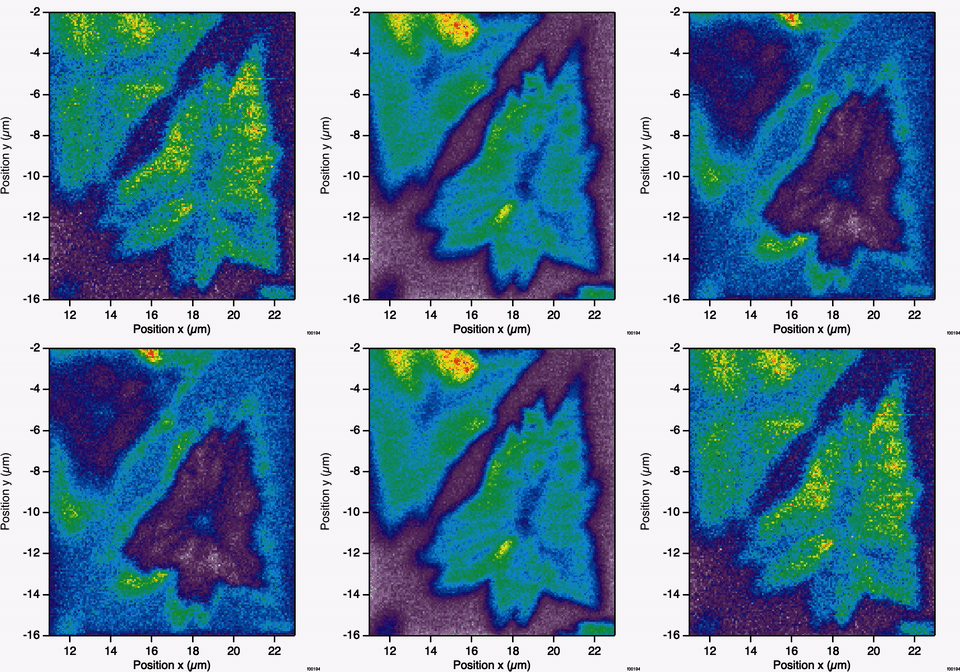
This animation displays a scan of arrow-shaped flakes of a 2D material. Samples were scanned across their electron energy, momentum, and horizontal and vertical coordinates using an X-ray-based technique known as nanoARPES at Berkeley Lab’s Advanced Light Source. Red represents the highest intensity measured, followed by orange, yellow, green, blue, and purple (least intense). (Credit: Roland Koch/Berkeley Lab)
Nothing is perfect, or so the saying goes, and that’s not always a bad thing. In a study at the Department of Energy’s Lawrence Berkeley National Laboratory (Berkeley Lab), scientists learned how nanoscale defects can enhance the properties of an ultrathin, so-called 2D material.
They combined a toolbox of techniques to home in on natural, nanoscale defects formed in the manufacture of tiny flakes of a monolayer material known as tungsten disulfide (WS2) and measured their electronic effects in detail not possible before.
“Usually we say that defects are bad for a material,” said Christoph Kastl, a postdoctoral researcher at Berkeley Lab’s Molecular Foundry and the lead author of the study, published in the journal ACS Nano. “Here they provide functionality.”
Tungsten disulfide is a well-studied 2D material that, like other 2D materials of its kind, exhibits special properties because of its atomic thinness. It is particularly well-known for its efficiency in absorbing and emitting light, and it is a semiconductor.
Members of this family of 2D materials could serve as high-efficiency computer transistors and as other electronics components, and they also are prime candidates for use in ultrathin, high-efficiency solar cells and LED lighting, as well as in quantum computers.
These 2D materials could also be incorporated in new forms of memory storage and data transfer, such as spintronics and valleytronics, that would revolutionize electronics by making use of materials in new ways to make smaller and more efficient devices.
The latest result marks the first comprehensive study at the Lab’s Advanced Light Source (ALS) involving a technique called nanoARPES, which researchers enlisted to probe the 2D samples with X-rays. The X-rays knocked out electrons in the sample, allowing researchers to measure their direction and energy. This revealed nanoscale defects and how the electrons interact with each other.
The nanoARPES capability is housed in an X-ray beamline, launched in 2016, known as MAESTRO (Microscopic and Electronic Structure Observatory). It is one of dozens of specialized beamlines at the ALS, which produces light in different forms – from infrared to X-rays – for a variety of simultaneous experiments.
“It’s a very big advance to get this electronic structure on small length scales,” said Eli Rotenberg, a senior staff scientist at the ALS who was a driving force in developing MAESTRO and served as one of the study’s leaders. “That matters for real devices.”
The team also enlisted a technique known as XPS (X-ray photoelectron spectroscopy) to study the chemical makeup of a sample at very small scales; a form of AFM (atomic force microscopy) to view structural details approaching the atomic scale; and a combined form of optical spectroscopy (Raman/photoluminescence spectroscopy) to study how light interacts with the electrons at microscope scales.
The various techniques were applied at the Molecular Foundry, where the material was synthesized, and at the ALS. The sample used in the study contained microscopic, roughly triangular flakes, each measuring about 1 to 5 microns (millionths of a meter) across. They were grown atop titanium dioxide crystals using a conventional layering process known as chemical vapor deposition, and the defects were largely concentrated around the edges of the flakes, a signature of the growth process. Most of the experiments focused on a single flake of tungsten disulfide.

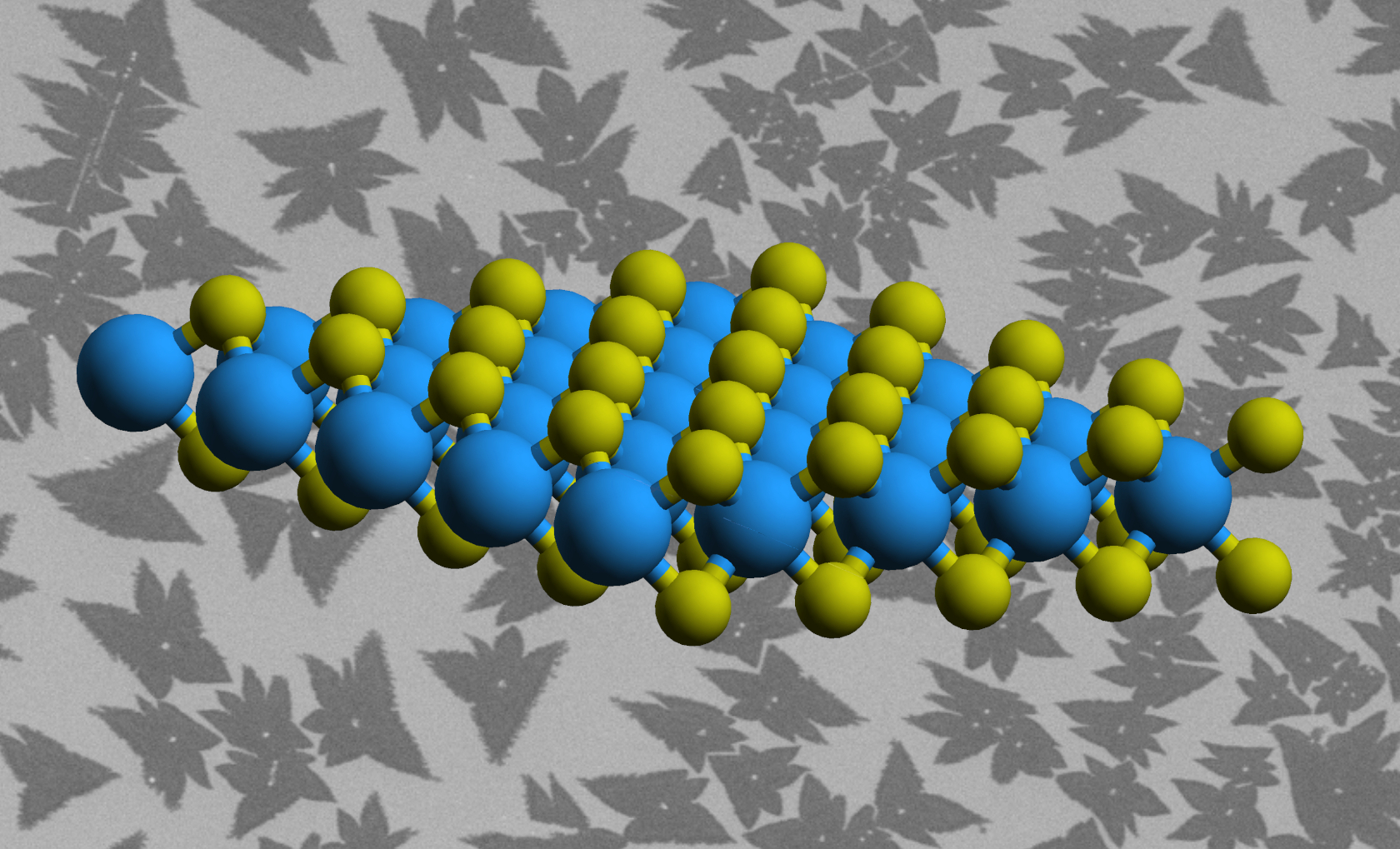
This image shows an illustration of the atomic structure of a 2D material called tungsten disulfide. Tungsten atoms are shown in blue and sulfur atoms are shown in yellow. The background image, taken by an electron microscope at Berkeley Lab’s Molecular Foundry, shows groupings of flakes of the material (dark gray) grown by a process called chemical vapor deposition on a titanium dioxide layer (light gray). (Credit: Katherine Cochrane/Berkeley Lab)
Adam Schwartzberg, a staff scientist at the Molecular Foundry who served as a co-lead in the study, said, “It took a combination of multiple types of techniques to pin down what’s really going on.”
He added, “Now that we know what defects we have and what effect they have on the properties of the material, we can use this information to reduce or eliminate defects – or if you want the defect, it gives us a way of knowing where the defects are,” and provides fresh insight about how to propagate and amplify the defects in the sample-production process.
While the concentration of edge defects in the WS2 flakes was generally known before the latest study, Schwartzberg said that their effects on materials performance hadn’t previously been studied in such a comprehensive and detailed way.
Researchers learned that a 10 percent deficiency in sulfur atoms was associated with the defective edge regions of the samples compared to other regions, and they identified a slighter, 3 percent sulfur deficiency toward the center of the flakes. Researchers also noted a change in the electronic structure and higher abundance of freely moving electrical charge-carriers associated with the high-defect edge areas.

This sequence of images shows a variety of energy intensities (white and yellow) at the edges of a 2D material known as tungsten disulfide, as measured via different techniques: photoluminescense intensity (far left); contact potential difference map (second from left); exciton emission intensity (third from left) – excitons are pairs consistent of an electrons and their quasiparticle counterpart, called a hole; trion emission intensity (far right) – trions are gropus of three charged quasiparticles consistening of either two electrons and a hole or two holes and an electron). (Credit: Christoph Kastl/Berkeley Lab)
For this study, the defects were due to the sample-growth process. Future nanoARPES studies will focus on samples with defects that are induced through chemical processing or other treatments. Researchers hope to control the amount and kinds of atoms that are affected, and the locations where these defects are concentrated in the flakes.
Such tiny tweaks could be important for processes like catalysis, which is used to enhance and accelerate many important industrial chemical production processes, and to explore quantum processes that rely on the production of individual particles that serve as information carriers in electronics.
Because research of WS2 and related 2D materials is still in its infancy, there are many unknowns about the roles specific types of defects play in these materials, and Rotenberg noted that there is a world of possibilities for so-called “defect engineering” in these materials.
In addition, MAESTRO’s nanoARPES has the ability to study the electronic structures of stacks of different types of 2D material layers. This can help researchers understand how their properties depend on their physical arrangement, and to explore working devices that incorporate 2D materials.
“The unprecedented small scale of the measurements – currently approaching 50 nanometers – makes nanoARPES a great discovery tool that will be particularly useful to understand new materials as they are invented,” Rotenberg said.
MAESTRO is one of the priority beamlines to be upgraded as part of the Lab’s ALS Upgrade (ALS-U) project, a major undertaking that will produce even brighter, more focused beams of light for experiments. “The ALS-U project will further improve the performance of the nanoARPES technique,” Rotenberg said, “making its measurements 10 to 30 times more efficient and significantly improving our ability to reach even shorter length scales.”
NanoARPES could play an important role in the development of new solar technologies, because it allows researchers to see how nanoscale variations in chemical makeup, number of defects, and other structural features affect the electrons that ultimately govern their performance. These same issues are important for many other complex materials, such as superconductors, magnets, and thermoelectrics – which convert temperature to current and vice versa – so nanoARPES will also be very useful for these as well.
The Molecular Foundry and ALS are both DOE Office of Science User Facilities.
Researchers from the Berkeley Lab Chemical Sciences Division, Aarhus University in Denmark, and Montana State University also participated in this study. The work was supported by the U.S. Department of Energy’s Office of Basic Energy Sciences, the DOE Early Career Grant program, Berkeley Lab’s Laboratory Directed Research and Development program, the Villum Foundation, and the German Academic Exchange Service.
# # #
Founded in 1931 on the belief that the biggest scientific challenges are best addressed by teams, Lawrence Berkeley National Laboratory and its scientists have been recognized with 13 Nobel Prizes. Today, Berkeley Lab researchers develop sustainable energy and environmental solutions, create useful new materials, advance the frontiers of computing, and probe the mysteries of life, matter, and the universe. Scientists from around the world rely on the Lab’s facilities for their own discovery science. Berkeley Lab is a multiprogram national laboratory, managed by the University of California for the U.S. Department of Energy’s Office of Science.
DOE’s Office of Science is the single largest supporter of basic research in the physical sciences in the United States, and is working to address some of the most pressing challenges of our time. For more information, please visit science.energy.gov.