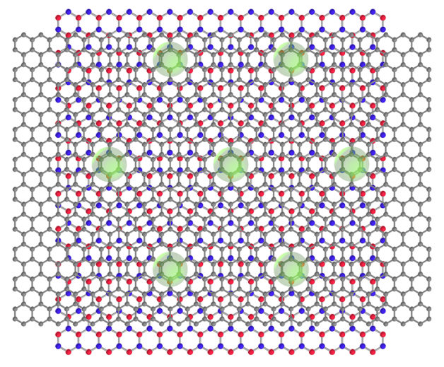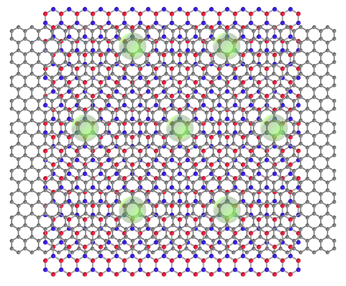
Schematic of graphene/boron nitride superconductor/insulator: The material is composed of three 2D layers of graphene (gray) sandwiched between 2D layers of boron nitride (red and blue) to form a repeating pattern called a moiré superlattice. Superconductivity is indicated by the light-green circles, which represent the positive charge sitting on each unit cell of the moiré superlattice. (Credit: Guorui Chen/Berkeley Lab)
What’s thinner than a human hair but has a depth of special traits? A multitasking graphene device developed by researchers at the U.S. Department of Energy’s Lawrence Berkeley National Laboratory (Berkeley Lab). The superthin material easily switches from a superconductor that conducts electricity without losing any energy, to an insulator that resists the flow of electric current, and back again to a superconductor – all with a simple flip of a switch. Their findings were reported today in the journal Nature.
“Usually, when someone wants to study how electrons interact with each other in a superconducting quantum phase versus an insulating phase, they would need to look at different materials. With our system, you can study both in one place,” said Guorui Chen, the study’s lead author and a postdoctoral researcher in the lab of Feng Wang, who led the study. Wang, a faculty scientist in Berkeley Lab’s Materials Sciences Division, is also a UC Berkeley physics professor.
The graphene device is composed of three atomically thin (2D) layers of graphene. When sandwiched between 2D layers of boron nitride, they form a repeating pattern called a moiré superlattice. The material could help other scientists understand the complicated mechanics behind a phenomenon known as high-temperature superconductivity, where a material can conduct electricity without resistance at temperatures higher than expected, though still hundreds of degrees below freezing.
In a previous study, the researchers reported observing the properties of a Mott insulator in a device made of trilayer graphene. A Mott insulator is a class of material that somehow stops conducting electricity at hundreds of degrees below freezing despite classical theory predicting electrical conductivity. But it has long been believed that a Mott insulator can become superconductive by adding more electrons or positive charges to make it superconductive, Chen explained.
For the past 10 years, scientists have been studying ways to combine different 2D materials, often starting with graphene – a material known for its ability to efficiently conduct heat and electricity. Out of this body of work, it was discovered that moiré superlattices formed with graphene exhibit exotic physics such as superconductivity when the layers are aligned at just the right angle.
“So for this study we asked ourselves, ‘If our trilayer graphene system is a Mott insulator, could it also be a superconductor?’” said Chen.
Opening the gate to a new world of physics

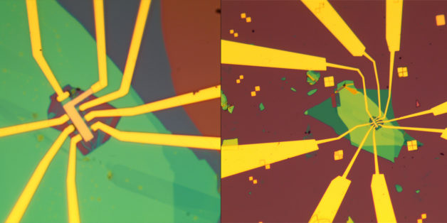
Two views of the trilayer graphene/boron nitride heterostructure device as seen through an optical microscope. The gold, nanofabricated electric contacts are shown in yellow; the silicon dioxide/silicon substrate is shown in brown; and the boron nitride flakes are shown in green. The trilayer graphene device – which is thinner than a human hair – is encapsulated between two boron nitride flakes. (Credit: Guorui Chen/Berkeley Lab)
Working with David Goldhaber-Gordon of Stanford University and the Stanford Institute for Materials and Energy Sciences at SLAC National Accelerator Laboratory, and Yuanbo Zhang of Fudan University, the researchers used a dilution refrigerator, which can reach intensely cold temperatures of 40 millikelvins – or nearly minus 460 degrees Fahrenheit – to cool the graphene/boron nitride device down to a temperature at which the researchers expected superconductivity to appear near the Mott insulator phase, said Chen.
Once the device reached a temperature of 4 kelvins (minus 452 degrees Fahrenheit), the researchers applied a range of electrical voltages to the tiny top and bottom gates of the device. As they expected, when they applied a high vertical electrical field to both the top and bottom gates, an electron filled each cell of the graphene/boron nitride device. This caused the electrons to stabilize and stay in place, and this “localization” of electrons turned the device into a Mott insulator.
Then, they applied an even higher electrical voltage to the gates. To their delight, a second reading indicated that the electrons were no longer stable. Instead, they were shuttling about, moving from cell to cell, and conducting electricity without loss or resistance. In other words, the device had switched from the Mott insulator phase to the superconductor phase.
Chen explained that the boron nitride moiré superlattice somehow increases the electron-electron interactions that take place when an electrical voltage is applied to the device, an effect that switches on its superconducting phase. It’s also reversible – when a lower electrical voltage is applied to the gates, the device switches back to an insulating state.
The multitasking device offers scientists a tiny, versatile playground for studying the exquisite interplay between atoms and electrons in exotic new superconducting materials with potential use in quantum computers – computers that store and manipulate information in qubits, which are typically subatomic particles such as electrons or photons – as well as new Mott insulator materials that could one day make tiny 2D Mott transistors for microelectronics a reality.
“This result was very exciting for us. We never imagined that the graphene/boron nitride device would do so well,” Chen said. “You can study almost everything with it, from single particles to superconductivity. It’s the best system I know of for studying new kinds of physics,” Chen said.
This study was supported by the Center for Novel Pathways to Quantum Coherence in Materials (NPQC), an Energy Frontier Research Center led by Berkeley Lab and funded by the DOE Office of Science. NPQC brings together researchers at Berkeley Lab, Argonne National Laboratory, Columbia University, and UC Santa Barbara to study how quantum coherence underlies unexpected phenomena in new materials such as trilayer graphene, with an eye toward future uses in quantum information science and technology.
Also contributing to the study were researchers from Shanghai Jiao Tong University and Nanjing University, China; the National Institute for Materials Science, Japan; and the University of Seoul, Korea.
###
Founded in 1931 on the belief that the biggest scientific challenges are best addressed by teams, Lawrence Berkeley National Laboratory and its scientists have been recognized with 13 Nobel Prizes. Today, Berkeley Lab researchers develop sustainable energy and environmental solutions, create useful new materials, advance the frontiers of computing, and probe the mysteries of life, matter, and the universe. Scientists from around the world rely on the Lab’s facilities for their own discovery science. Berkeley Lab is a multiprogram national laboratory, managed by the University of California for the U.S. Department of Energy’s Office of Science.
DOE’s Office of Science is the single largest supporter of basic research in the physical sciences in the United States, and is working to address some of the most pressing challenges of our time. For more information, please visit energy.gov/science.
