
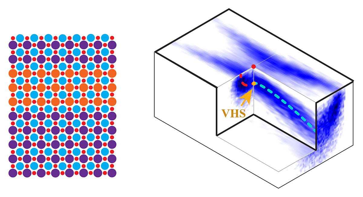
Right: Animation of a Van Hove singularity (VHS) shown approximately 1 nanometer below the surface of an oxide heterostructure made of atomically thin layers of strontium titanate and samarium titanate. Left: Atomic composition of the oxide heterostructure illustrated by colored dots: Purple represents samarium; orange represents strontium; light blue represents titanium; and small red dots represent oxygen. (Credit: Ryo Mori/Berkeley Lab)
In the search for new materials with the potential to outperform silicon, scientists have wanted to take advantage of the unusual electronic properties of 2D devices called oxide heterostructures, which consist of atomically thin layers of materials containing oxygen.
Scientists have long known that oxide materials, on their own, are typically insulating – which means that they are not electrically conductive. When two oxide materials are layered together to form a heterostructure, new electronic properties such as superconductivity – the state in which a material can conduct electricity without resistance, typically at hundreds of degrees below freezing – and magnetism somehow form at their interface, which is the juncture where two materials meet. But very little is known about how to control these electronic states because few techniques can probe below the interface.
Now, a team of researchers led by the Department of Energy’s Lawrence Berkeley National Laboratory (Berkeley Lab) has gained new insight into the evolution of exotic electronic properties from atomically thin oxide heterostructures. Their findings – reported in the journal Nature Communications – could lead to new electronic materials that surpass the limitations imposed by Moore’s Law, which predicted in 1975 that the number of transistors packed into a tiny silicon-based computer chip would double every two years.
At Berkeley Lab’s Advanced Light Source, the research team – directed by Alessandra Lanzara, senior faculty scientist in Berkeley Lab’s Materials Sciences Division and professor of physics at UC Berkeley – used a special technique called angle-resolved photoemission spectroscopy (ARPES) to directly measure the electronic structure of electrons confined between layers of a strontium titanate/samarium titanate heterostructure.
Probing at a depth of approximately 1 nanometer (a billionth of a meter) inside the sample, the researchers discovered two unique electronic properties – called a Van Hove singularity (VHS) and Fermi surface topology – which condensed matter physicists have long considered important features for tuning superconductivity and other such exotic electronic states in electronic materials.
The researchers’ observation of VHS and Fermi surface topology at the interface between atomically thin oxide materials for the first time suggests that the system is an ideal platform for investigating how to control superconductivity at the atomic scale in 2D materials.
“Our findings add new pieces of information to this young field. While the road toward the industrial use of oxide electronics is still far, our work is a step forward in the development of next-generation alternatives to traditional electronics beyond Moore’s Law,” said lead author Ryo Mori, a doctoral researcher in Berkeley Lab’s Materials Sciences Division and Ph.D. student in the Applied Science and Technology (AS&T) program at UC Berkeley.
The scientists next plan to further investigate how electronic properties such as Van Hove singularities change at higher temperatures and different voltages.
Researchers from Berkeley Lab, UC Berkeley, and UC Santa Barbara participated in the study.
The Advanced Light Source is a DOE Office of Science user facility at Berkeley Lab.
This work was supported by the DOE Office of Science. Additional funding was provided by the Gordon and Betty Moore Foundation and the National Science Foundation.
###
Founded in 1931 on the belief that the biggest scientific challenges are best addressed by teams, Lawrence Berkeley National Laboratory and its scientists have been recognized with 13 Nobel Prizes. Today, Berkeley Lab researchers develop sustainable energy and environmental solutions, create useful new materials, advance the frontiers of computing, and probe the mysteries of life, matter, and the universe. Scientists from around the world rely on the Lab’s facilities for their own discovery science. Berkeley Lab is a multiprogram national laboratory, managed by the University of California for the U.S. Department of Energy’s Office of Science.
DOE’s Office of Science is the single largest supporter of basic research in the physical sciences in the United States, and is working to address some of the most pressing challenges of our time. For more information, please visit energy.gov/science.