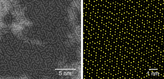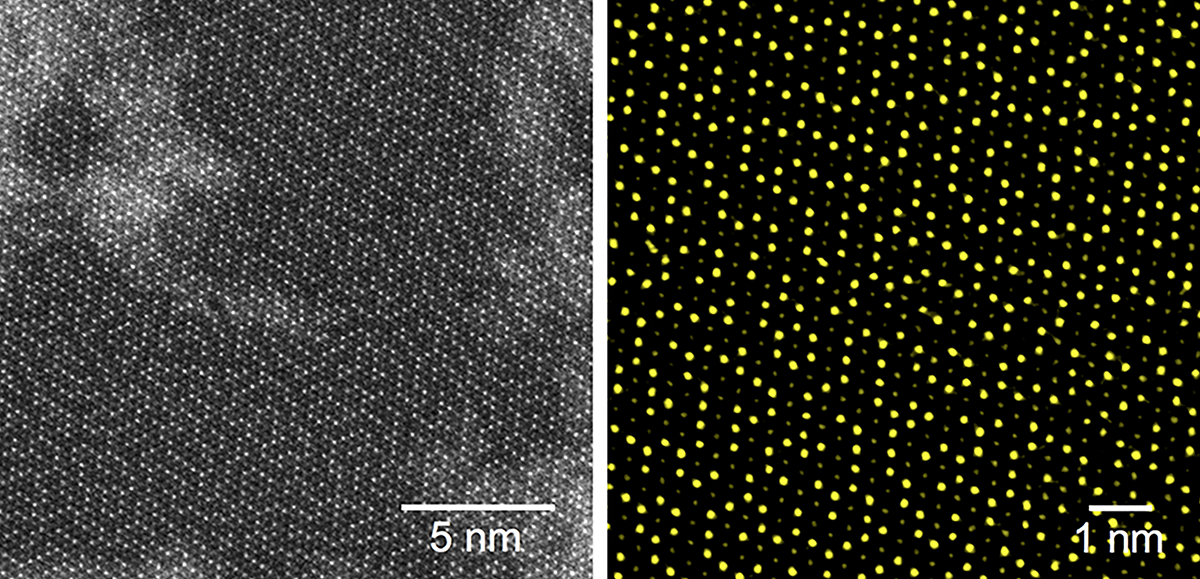
Electron microscopy experiments revealed meandering stripes formed by metal atoms of rhenium and niobium in the lattice structure of a 2D transition metal dichalcogenide alloy. (Image courtesy of Amin Azizi)
To tune the band gap, a key parameter in controlling the electrical conductivity and optical properties of semiconductors, researchers typically engineer alloys, a process in which two or more materials are combined to achieve properties that otherwise could not be achieved by a pristine material.
But engineering band gaps of conventional semiconductors via alloying has often been a guessing game, because scientists have not had a technique to directly “see” whether the alloy’s atoms are arranged in a specific pattern, or randomly dispersed.
Now, as reported in Physical Review Letters, a research team led by Alex Zettl and Marvin Cohen – senior faculty scientists in the Materials Sciences Division at the Department of Energy’s Lawrence Berkeley National Laboratory (Berkeley Lab), and professors of physics at UC Berkeley – has demonstrated a new technique that could engineer the band gap needed to improve the performance of semiconductors for next-generation electronics such as optoelectronics, thermoelectrics, and sensors.
For the current study, the researchers examined monolayer and multilayer samples of a 2D transition metal dichalcogenide (TMD) material made of the alloy rhenium niobium disulfide.
Electron microscopy experiments revealed meandering stripes formed by metal atoms of rhenium and niobium in the lattice structure of the 2D TMD alloy.
A statistical analysis confirmed what the research team had suspected – that metal atoms in the 2D TMD alloy prefer to be adjacent to the other metal atoms, “which is in stark contrast to the random structure of other TMD alloys of the same class,” said lead author Amin Azizi, a postdoctoral researcher in the Zettl lab at UC Berkeley.
Calculations performed at Berkeley Lab’s National Energy Research Scientific Computing Center (NERSC) by Mehmet Dogan, a postdoctoral researcher in the Cohen lab at UC Berkeley, demonstrated that such atomic ordering can modify the material’s band gap.
Optical spectroscopy measurements performed at Berkeley Lab’s Advanced Light Source revealed that the band gap of the 2D TMD alloy can be additionally tuned by adjusting the number of layers in the material. Also, the band gap of the monolayer alloy is similar to that of silicon – which is “just right” for many electronic and optical applications, Azizi said. And the 2D TMD alloy has the added benefits of being flexible and transparent.
The researchers next plan to explore the sensing and optoelectronic properties of new devices based on the 2D TMD alloy.
Co-authors with Azizi, Cohen, and Zettl include Jeffrey D. Cain, Mehmet Dogan, Rahmatollah Eskandari, Emily G. Glazer, and Xuanze Yu.
The Advanced Light Source and NERSC are DOE Office of Science user facilities co-located at Berkeley Lab.
This work was supported by the DOE Office of Science. Additional funding was provided by the National Science Foundation.
###
Founded in 1931 on the belief that the biggest scientific challenges are best addressed by teams, Lawrence Berkeley National Laboratory and its scientists have been recognized with 13 Nobel Prizes. Today, Berkeley Lab researchers develop sustainable energy and environmental solutions, create useful new materials, advance the frontiers of computing, and probe the mysteries of life, matter, and the universe. Scientists from around the world rely on the Lab’s facilities for their own discovery science. Berkeley Lab is a multiprogram national laboratory, managed by the University of California for the U.S. Department of Energy’s Office of Science.
DOE’s Office of Science is the single largest supporter of basic research in the physical sciences in the United States, and is working to address some of the most pressing challenges of our time. For more information, please visit energy.gov/science.
