STEM (scanning transmission electron microscopy) image of a one-dimensional array of F4TCNQ molecules (yellow-orange) on a gate-tunable graphene device. (Credit: Berkeley Lab)
Small electronic circuits power our everyday lives, from the tiny cameras in our phones to the microprocessors in our computers. To make those devices even smaller, scientists and engineers are designing circuitry components out of single molecules. Not only could miniaturized circuits offer the benefits of increased device density, speed, and energy efficiency – for example in flexible electronics or in data storage – but harnessing the physical properties of specific molecules could lead to devices with unique functionalities. However, developing practical nanoelectronic devices from single molecules requires precise control over the electronic behavior of those molecules, and a reliable method by which to fabricate them.
Now, as reported in the journal Nature Electronics, researchers have developed a method to fabricate a one-dimensional array of individual molecules and to precisely control its electronic structure. By carefully tuning the voltage applied to a chain of molecules embedded in a one-dimensional carbon (graphene) layer, the team led by researchers at Lawrence Berkeley National Laboratory (Berkeley Lab) found it could control whether all, none, or some of the molecules carry an electric charge. The resulting charge pattern could then be shifted along the chain by manipulating individual molecules at the end of the chain.
“If you’re going to build electrical devices out of individual molecules, you need molecules that have useful functionality and you need to figure out how to arrange them in a useful pattern. We did both of those things in this work,” said Michael Crommie, a senior faculty scientist in Berkeley Lab’s Materials Sciences Division, who led the project. The research is part of a U.S. Department of Energy (DOE) Office of Science-funded program on Characterization of Functional Nanomachines, whose overarching goal is to understand the electrical and mechanical properties of molecular nanostructures, and to create new molecule-based nanomachines capable of converting energy from one form to another at the nanoscale.
The key trait of the fluorine-rich molecule selected by the Berkeley Lab team is its strong tendency to accept electrons. To control the electronic properties of a precisely aligned chain of 15 such molecules deposited on a graphene substrate, Crommie, who is also a UC Berkeley professor of physics, and his colleagues placed a metallic electrode underneath the graphene that was also separated from it by a thin insulating layer. Applying a voltage between the molecules and the electrode drives electrons into or out of the molecules. In that way, the graphene-supported molecules behave somewhat like a capacitor, an electrical component used in a circuit to store and release charge. But, unlike a “normal” macroscopic capacitor, by tuning the voltage on the bottom electrode the researchers could control which molecules became charged and which remained neutral.

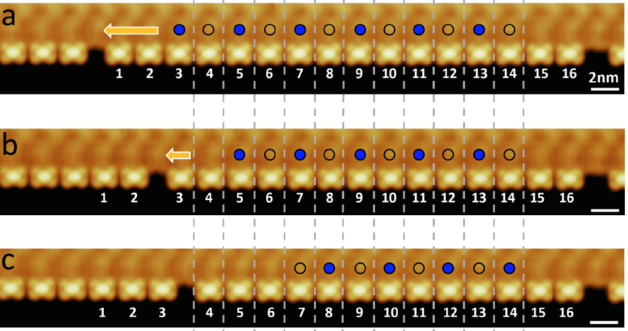
A one-dimensional array of molecules switch from electrically charged (blue dot) to neutral (empty dot) when an odd number of molecules is removed from the end of the pattern. This forces an electron into what used to be the second-to-the-last molecule, causing the other molecules to switch their charge state, thus shifting the alternating pattern of charges. (Berkeley Lab)
In previous studies of molecular assemblies, the molecules’ electronic properties could not be both tuned and imaged at atomic length scales. Without the additional imaging capability the relationship between structure and function cannot be fully understood in the context of electrical devices. By placing the molecules in a specially designed template on the graphene substrate developed at Berkeley Lab’s Molecular Foundry nanoscale science user facility, Crommie and his colleagues ensured that the molecules were completely accessible to both microscope observation and electrical manipulation.
As expected, applying a strong positive voltage to the metallic electrode underneath the graphene supporting the molecules filled them with electrons, leaving the entire molecular array in a negatively charged state. Removing or reversing that voltage caused all the added electrons to leave the molecules, returning the entire array to a charge neutral state. At an intermediate voltage, however, electrons fill only every other molecule in the array, thus creating a “checkerboard” pattern of charge. Crommie and his team explain this novel behavior by the fact that electrons repel each other. If two charged molecules were to momentarily occupy adjacent sites, then their repulsion would push one of the electrons away and force it to settle one site farther down the molecular row.
“We can make all the molecules empty of charge, or all full, or alternating. We call that a collective charge pattern because it’s determined by electron-electron repulsion throughout the structure,” said Crommie.
Calculations suggested that in an array of molecules with alternating charges the terminal molecule in the array should always contain one extra electron since that molecule does not have a second neighbor to cause repulsion. In order to experimentally investigate this type of behavior, the Berkeley Lab team removed the final molecule in an array of molecules that had alternating charges. They found that the original charge pattern had shifted over by one molecule: sites that had been charged became neutral and vice versa. The researchers concluded that before the charged terminal molecule was removed, the molecule adjacent to it must have been neutral. In its new position at the end of the array, the formerly second molecule then became charged. To maintain the alternating pattern between charged and uncharged molecules, the entire charge pattern had to shift by one molecule.
If the charge of each molecule is thought of as a bit of information, then removing the final molecule causes the entire pattern of information to shift by one position. That behavior mimics an electronic shift register in a digital circuit and provides new possibilities for transmitting information from one region of a molecular device to another. Moving a molecule at one end of the array could serve as flipping a switch on or off somewhere else in the device, providing useful functionality for a future logic circuit.
“One thing that we found really interesting about this result is that we were able to alter the electronic charge and therefore the properties of molecules from very far away. That level of control is something new,” said Crommie.
With their molecular array the researchers achieved the goal of creating a structure that has very specific functionality; that is, a structure whose molecular charges may be finely tuned between different possible states by applying a voltage. Changing the charge of the molecules causes a change in their electronic behavior and, as a result, in the functionality of the entire device. This work came out of a DOE effort to construct precise molecular nanostructures that have well-defined electromechanical functionality.
The Berkeley Lab team’s technique for controlling molecular charge patterns could lead to new designs for nanoscale electronic components including transistors and logic gates. The technique could also be generalized to other materials and incorporated into more complex molecular networks. One possibility is to tune the molecules to create more complex charge patterns. For example, replacing one atom with another in a molecule can change the molecule’s properties. Placing such altered molecules in the array could create new functionality. Based on these results the researchers plan to explore the functionality that arises from new variations within molecular arrays, as well as how they can potentially be used as tiny circuit components. Ultimately, they plan to incorporate these structures into more practical nanoscale devices.
The Molecular Foundry is a DOE Office of Science user facility located at Berkeley Lab.
# # #
Founded in 1931 on the belief that the biggest scientific challenges are best addressed by teams, Lawrence Berkeley National Laboratory and its scientists have been recognized with 14 Nobel Prizes. Today, Berkeley Lab researchers develop sustainable energy and environmental solutions, create useful new materials, advance the frontiers of computing, and probe the mysteries of life, matter, and the universe. Scientists from around the world rely on the Lab’s facilities for their own discovery science. Berkeley Lab is a multiprogram national laboratory, managed by the University of California for the U.S. Department of Energy’s Office of Science.
DOE’s Office of Science is the single largest supporter of basic research in the physical sciences in the United States, and is working to address some of the most pressing challenges of our time. For more information, please visit energy.gov/science.
Media Contact:
[email protected]
510-486-5183
