Scientists at Berkeley Lab’s predecessor, the UC Radiation Laboratory, discovered berkelium in 1949, and californium in 1950. Today, Berkeley Lab scientists are using state-of-the-art instruments at the Molecular Foundry to better understand how actinides like berkelium and californium could serve to accelerate new applications in medicine, energy, and security. (Credit: Shutterstock/konstantinks)
H eavy elements known as the actinides are important materials for medicine, energy, and national defense. But even though the first actinides were discovered by scientists at Berkeley Lab more than 50 years ago, we still don’t know much about their chemical properties because only small amounts of these highly radioactive elements (or isotopes) are produced every year; they’re expensive; and their radioactivity makes them challenging to handle and store safely.
But those massive hurdles to actinide research may one day be a thing of the past. Scientists at the U.S. Department of Energy’s Lawrence Berkeley National Laboratory (Berkeley Lab) and UC Berkeley have demonstrated how a world-leading electron microscope can image actinide samples as small as a single nanogram (a billionth of a gram) – a quantity that is several orders of magnitude less than required by conventional approaches.
Their findings were recently reported in Nature Communications, and are especially significant for co-senior author Rebecca Abergel, whose work on chelators – metal-binding molecules – has resulted in new advances in cancer therapies, medical imaging, and medical countermeasures against nuclear threats, among others. Abergel is a faculty scientist who leads the Heavy Element Chemistry program in the Chemical Sciences Division at Berkeley Lab, and assistant professor in nuclear engineering at UC Berkeley.
“There are still so many unanswered questions with regards to chemical bonding in the actinide series. With such state-of-the art instrumentation, we are finally able to probe the electronic structure of actinide compounds, and this will allow us to refine molecular design principles for various systems with applications in medicine, energy, and security,” Abergel said.
“We demonstrated that you can work with less material – a nanogram – and get the same if not better data without having to invest in dedicated instruments for radioactive materials,” said co-senior author Andy Minor, facility director of the National Center for Electron Microscopy at Berkeley Lab’s Molecular Foundry, and professor of materials science and engineering at UC Berkeley.

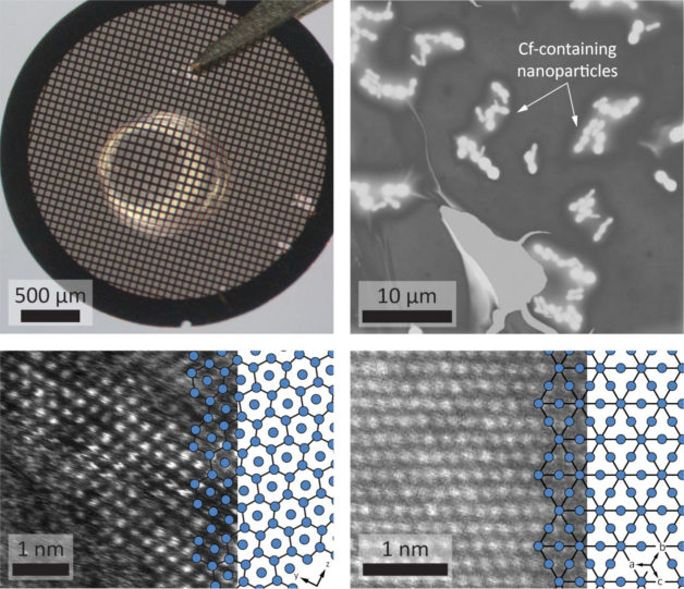
Top: (left) Droplet of solution containing californium on a transmission electron microscopy (TEM) grid; (right) scanning electron microscopy (SEM) image of individual californium-containing nanoparticles. Bottom: scanning transmission electron microscopy (STEM) images of crystal structures of (left) Cf2O3 – blue schematic outlines californium columns; and (right) BkO2 – blue schematic illustrates berkelium lattice. (Credit: Andy Minor and Rebecca Abergel/Berkeley Lab)
Allowing researchers to work with just a nanogram of an actinide sample will significantly reduce the high costs of experiments conducted using previous methods. One gram of the actinide berkelium can cost a jaw-dropping $27 million, for example. An actinide sample that is only a nanogram also reduces radiation exposure and contamination risks, Minor added.
In one set of experiments at TEAM 0.5 (Transmission Electron Aberration-corrected Microscope), an atomic-resolution electron microscope at the Molecular Foundry, the researchers imaged single atoms of berkelium and californium to demonstrate how much less actinide material is needed with their approach.
In another set of experiments using EELS (electron energy loss spectroscopy), a technique for probing a material’s electronic structure, the researchers were surprised to observe in berkelium a weak “spin-orbit coupling,” a phenomenon that can influence how a metal atom binds to molecules. “This had never been reported before,” said co-author Peter Ercius, a staff scientist at the Molecular Foundry who oversees the TEAM 0.5 microscope. “It’s like finding a needle in a haystack. It’s amazing what we could see.”
Co-lead author Alexander Müller credits Berkeley Lab’s interdisciplinary “team science” approach for bringing together the world’s best experts in electron microscopy, heavy element chemistry, nuclear engineering, and materials science for the study.
“Because Berkeley Lab attracts amazing researchers from all fields of science, such interdisciplinary collaborative work comes naturally here,” he said. “I personally found that aspect very rewarding for this project. And now that we have established this approach, we can pursue many new directions in actinide research.” Müller was a postdoctoral scholar in Berkeley Lab’s Molecular Foundry and UC Berkeley’s Department of Materials Science and Engineering at the time of the study. He is now an associate at the Munich, Germany, office of Kearney, an international management consulting firm.
Safety protocols in place for the research involved sample preparation in dedicated laboratories and careful surveying of work areas. Since samples were prepared with miniscule amounts (1-10 nanograms) of each isotope, the contamination hazards to the equipment were also minimized, the researchers said.
The researchers hope to apply their approach to the investigation of other actinides, including actinium, einsteinium, and fermium.
“The more information we get from these minute amounts of radioactive elements, the better equipped we’ll be to advance new materials for radiation cancer therapy and other useful applications,” Minor said.
Co-authors on the paper include former Berkeley Lab postdoctoral scholar Gauthier Deblonde (co-lead author), now a research scientist at Lawrence Livermore National Laboratory, and Steven Zeltmann, a graduate student in UC Berkeley’s Department of Materials Science and Engineering.
The Molecular Foundry is a DOE Office of Science user facility at Berkeley Lab.
The berkelium-249 and californium-249 chloride starting materials were supplied by the Isotope Program within the Office of Science.
This work was supported by the U.S. Department of Energy Office of Science. Additional funding was provided by the National Science Foundation’s STROBE Science and Technology Center“.
# # #
Founded in 1931 on the belief that the biggest scientific challenges are best addressed by teams, Lawrence Berkeley National Laboratory and its scientists have been recognized with 14 Nobel Prizes. Today, Berkeley Lab researchers develop sustainable energy and environmental solutions, create useful new materials, advance the frontiers of computing, and probe the mysteries of life, matter, and the universe. Scientists from around the world rely on the Lab’s facilities for their own discovery science. Berkeley Lab is a multiprogram national laboratory, managed by the University of California for the U.S. Department of Energy’s Office of Science.
DOE’s Office of Science is the single largest supporter of basic research in the physical sciences in the United States, and is working to address some of the most pressing challenges of our time. For more information, please visit energy.gov/science.
