
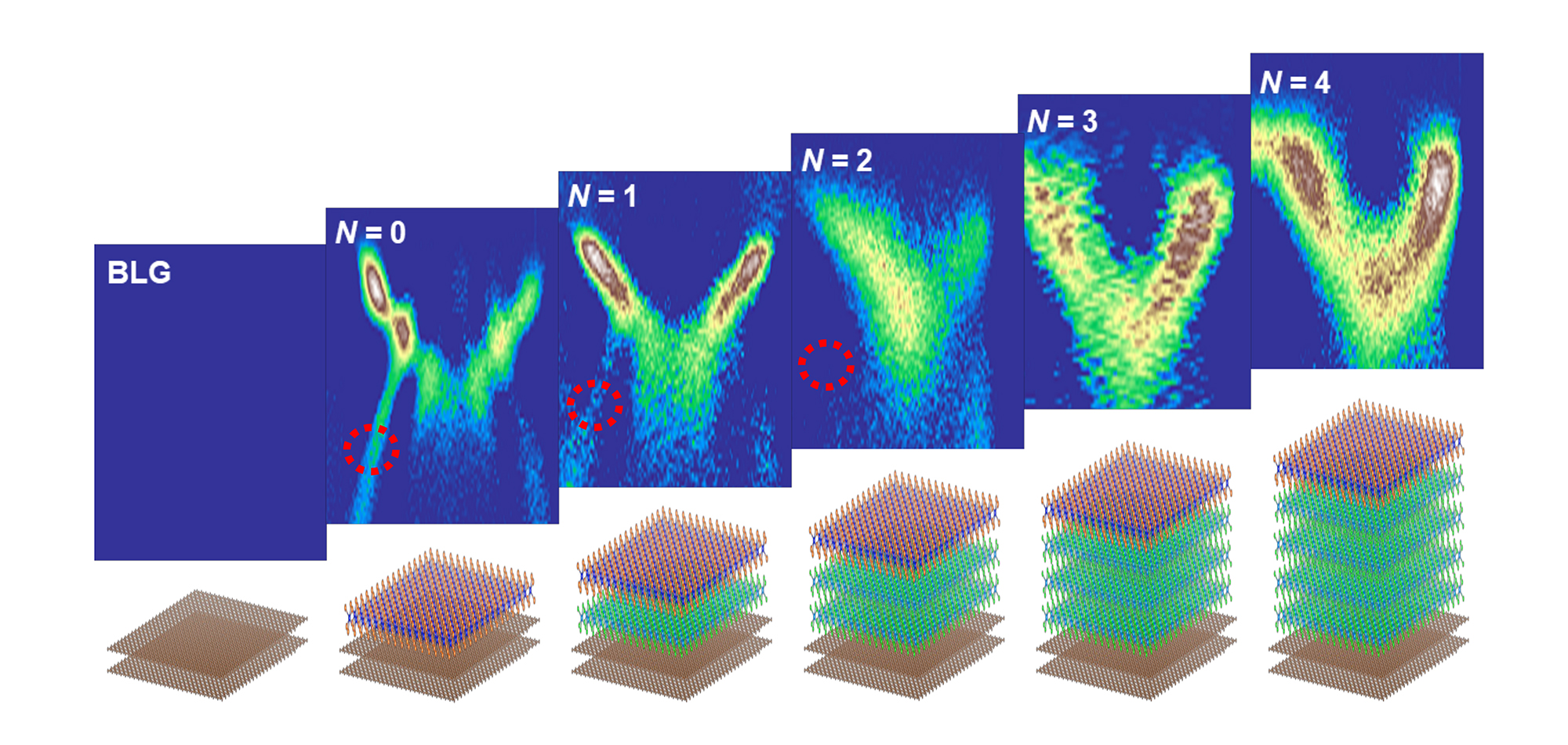
Using ultraviolet light, researchers probed the electronic characteristics of a 2D semiconductor (purple) as the number of substrate layers (green) increased. In the data maps, red circles mark an electronic feature that diminished as substrate layers were added. (Credit: Meng Kai Lin/University of Illinois at Urbana-Champaign)
Atomically thin layers are of great technological interest because of potentially useful electronic properties that emerge as the layer thickness approaches the 2D limit. Such materials tend to form weak bonds outside the layer and are thus generally assumed to be unaffected by substrates that provide physical support.
To make further progress, however, scientists must rigorously test this assumption, not only to better understand single-layer physics, but also because the existence of substrate effects raises the possibility of tuning layer properties by tweaking the substrate.
As reported in the journal Physical Review Letters, a team led by Tai-Chang Chiang of the University of Illinois at Urbana-Champaign and his postdoctoral associate, Meng-Kai Lin, used Berkeley Lab’s Advanced Light Source (ALS) to probe changes in the electronic properties of a 2D semiconductor, titanium telluride, as the thickness of a substrate, platinum telluride, was increased. Single-layer titanium telluride is highly sensitive to what lies underneath, making it particularly useful as a test case for investigating substrate coupling effects.
The results showed that as the substrate thickness increased, a dramatic and systematic variation occurred in the single-layer titanium telluride. An electronic phenomenon known as a charge density wave — a coupled charge and lattice distortion characteristic of single-layer titanium telluride — was suppressed.
“The experimental findings, combined with first-principles theoretical simulations, led to a detailed explanation of the results in terms of the basic quantum mechanical interactions between the single layer and the tunable substrate,” said Lin.
Given that the interfacial bonding remained weak, the researchers concluded that the observed changes were correlated with the substrate’s transformation from a semiconductor to a semimetal as it increased in thickness.
“This systematic study illustrates the crucial role that substrate interactions play in the physics of ultrathin films,” said Lin. “The scientific understanding derived from our work also provides a framework for designing and engineering ultrathin films for useful and enhanced properties.”