
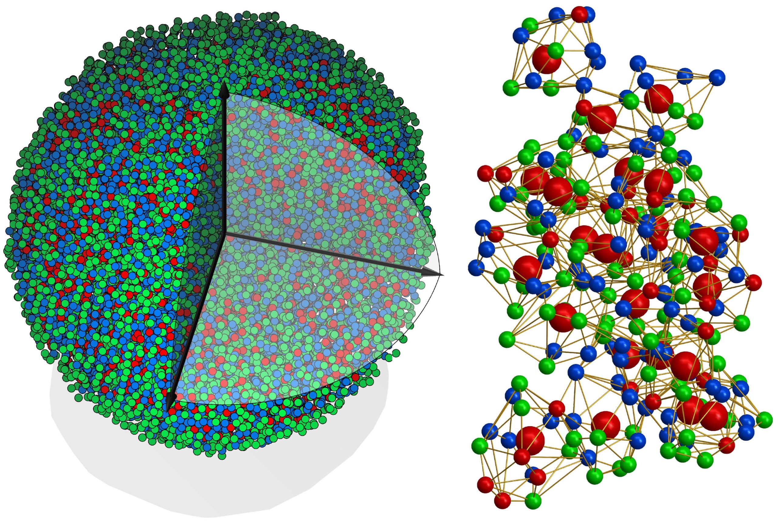
At left, an experimental 3D atomic model of a metallic glass nanoparticle, 8 nanometers in diameter. Right: The 3D atomic packing of a supercluster within the structure. Differently colored balls represent different types of atoms. Berkeley Lab scientists’ invention of the highly stable sample holder for the Molecular Foundry’s award-winning Transmission Electron Aberration-corrected Microscope (TEAM 0.5) helped lay the foundation for the achievement reported in the current study. (Courtesy of Yao Yang and Jianwei “John” Miao/UCLA)
Note: This press release has been adapted from an original UCLA release. View the original release.
Glass, rubber and plastics all belong to a class of matter called amorphous solids. And in spite of how common they are in our everyday lives, amorphous solids have long posed a challenge to scientists.
Since the 1910s, scientists have been able to map in 3D the atomic structures of crystals, the other major class of solids, which has led to myriad advances in physics, chemistry, biology, materials science, geology, nanoscience, drug discovery and more. But because amorphous solids aren’t assembled in rigid, repetitive atomic structures like crystals are, they have defied researchers’ ability to determine their atomic structure with the same level of precision.
Now, a UCLA-led study in collaboration with the Molecular Foundry, a nanoscience user facility at the U.S. Department of Energy’s Lawrence Berkeley National Laboratory (Berkeley Lab), reports on the first-ever determination of the 3D atomic structure of an amorphous solid – in this case, a material called metallic glass. Their findings were reported in the journal Nature.
“We combined state-of-the-art electron microscopy with powerful algorithms and analysis techniques to study structures down to the level of single atoms,” said co-author Peter Ercius, a staff scientist at the Molecular Foundry, where the experiment was conducted. “This is very similar to a medical CT (computed tomography) scan – except at the atomic level. Direct knowledge of amorphous structures at this level is a game changer for the physical sciences.”
“We know so much about crystals, yet most of the matter on Earth is non-crystalline and we know so little about their atomic structure,” said the study’s senior author, Jianwei “John” Miao, a UCLA professor of physics and astronomy and member of the California NanoSystems Institute at UCLA.
Observing the 3D atomic arrangement of an amorphous solid has been Miao’s dream since he was a graduate student. That dream has now been realized, after 22 years of relentless pursuit.
“This study just opened a new door,” he said.
Metallic glasses tend to be both stronger and more shapeable than standard crystalline metals, and they are used today in products ranging from electrical transformers to high-end golf clubs and the housings for Apple laptops and other electronic devices. Understanding the atomic structure of metallic glasses could help engineers design even better versions of these materials, for an even wider array of applications.
The researchers used a technique called atomic electron tomography, a type of 3D imaging pioneered by Miao’s group at UCLA and staff scientists in the National Center for Electron Microscopy, a facility at the Molecular Foundry. The approach involves beaming electrons through a sample and collecting an image on the other side. The sample is rotated so that measurements can be taken from multiple angles, yielding data that is stitched together to produce a 3D image.
The researchers examined a sample of metallic glass about 8 nanometers in diameter, made of eight different metals. (A nanometer is one-billionth of a meter.) Using 55 atomic electron tomography images, the researchers created a 3D map of the approximately 18,000 atoms that made up the nanoparticle.
Because amorphous solids have been so difficult to characterize, the researchers expected the atoms to be arranged chaotically. And although about 85% of the atoms were in a disordered arrangement, the researchers were able to identify pockets where a fraction of atoms coalesced into ordered superclusters. The finding demonstrated that even within an amorphous solid, the arrangement of atoms is not completely random.
Some of the metal atoms were so similar in size that electron imaging couldn’t distinguish between them. For the purposes of the study, the researchers grouped the metals into three categories, uniting neighbors from the periodic table of elements: cobalt and nickel in the first category; ruthenium, rhodium, palladium and silver in the second; and iridium and platinum in the third.
“All properties of any material come from how the atoms are arranged together, and one vexing goal has been to image the 3D atomic structure of a material that is completely disordered,” said co-author Andreas Schmid, whose invention of the highly stable sample holder for the Molecular Foundry’s award-winning Transmission Electron Aberration-corrected Microscope (TEAM 0.5) helped lay the foundation for the achievement reported in the current study. “This really is a breakthrough. It’s exciting to see that we have finally achieved 3D atomic imaging of an amorphous material.”
Ercius attributes the current study’s success to the TEAM microscopes and to Berkeley Lab’s decades of experience in pushing the limits of electron tomography toward atomic resolution. Now that they have demonstrated 3D atomic imaging of a metallic glass, Ercius would like to use the technique to image the atoms of other amorphous materials – or atomic defects in metals for quantum information systems: “In a transistor or quantum qubit, how do we know which defects are good for performance, and which ones are bad? With this technique, we could potentially find out, and push the limits of Moore’s Law.”
The Molecular Foundry is a DOE Office of Science user facility at Berkeley Lab.
The research was supported primarily by the STROBE National Science Foundation Science and Technology Center, of which Miao is deputy director, and in part by the U.S. Department of Energy.
###
Founded in 1931 on the belief that the biggest scientific challenges are best addressed by teams, Lawrence Berkeley National Laboratory and its scientists have been recognized with 14 Nobel Prizes. Today, Berkeley Lab researchers develop sustainable energy and environmental solutions, create useful new materials, advance the frontiers of computing, and probe the mysteries of life, matter, and the universe. Scientists from around the world rely on the Lab’s facilities for their own discovery science. Berkeley Lab is a multiprogram national laboratory, managed by the University of California for the U.S. Department of Energy’s Office of Science.
DOE’s Office of Science is the single largest supporter of basic research in the physical sciences in the United States, and is working to address some of the most pressing challenges of our time. For more information, please visit energy.gov/science.