Crystallization is one of the most fundamental processes found in nature – and it’s what gives minerals, gems, metals, and even proteins their structure.
In the past couple of decades, scientists have tried to uncover how natural crystals self-assemble and grow – and their pioneering work has led to some exciting new technologies – from the quantum dots behind colorful QLED TV displays, to peptoids, a protein-mimic that has inspired dozens of biotech breakthroughs.
Now, a research team led by scientists at the Department of Energy’s Lawrence Berkeley National Laboratory (Berkeley Lab) and UC Berkeley has developed a nanoparticle composite that grows into 3D crystals. The scientists say that the new material – which they call a 3D PGNP (polymer-grafted nanoparticle) crystal in their recently published Nature Communications study – could lead to new technologies that are 3D-grown rather than 3D-printed.
“We’ve demonstrated a new lever to turn, so to speak, to grow a crystalline material into a composite or structured material for applications ranging from nanoscale photonics for smart buildings to actuators for robotics,” said Ting Xu, senior author of the study. Xu is a faculty senior scientist in Berkeley Lab’s Materials Sciences Division and professor of chemistry and materials science and engineering at UC Berkeley.

A Nature Communications study led by Ting Xu (bottom right), faculty senior scientist in Berkeley Lab’s Materials Sciences Division and professor of chemistry and materials science and engineering at UC Berkeley, provides new clues into how crystals form at the atomic level. Lead author Yiwen Qian (bottom left) is a UC Berkeley graduate student researcher. Peter Ercius (top right) led the STEM tomography experiments at the Molecular Foundry. Yi Liu (top left), director of the Molecular Foundry’s Organic and Macromolecular Synthesis Facility, is a co-author of the study. (Credit: Marilyn Sargent/Berkeley Lab)
Xu said that their new method is compatible with the demands of mass manufacturing. “Many smart minds have designed elegant chemistries, such as DNAs and supramolecules, to crystallize nanoparticles. Our system is essentially a blend of nanoparticle and polymers – which are similar to the ingredients people use to make airplane wings or automobile bumpers. But what’s even more interesting is that we didn’t expect our method to be so simple and so fast,” Xu said.
A chance discovery
Lead author Yiwen Qian, a Ph.D. student researcher in the Xu Group at UC Berkeley, discovered the 3D PGNP nanocrystals by chance in an ordinary lab experiment.
A couple of days before, she had left a solution of toluene solvent and gold nanoparticles grafted with polystyrene (Au-PS) in a centrifuge tube on a lab counter. When she looked at the sample under a transmission electron microscope (TEM), she noticed something odd. “Nanoparticles had crystallized quickly. That was not a normal thing to expect,” she said.
To investigate, Xu collaborated with Peter Ercius, a staff scientist at Berkeley Lab’s Molecular Foundry, and Wolfgang Theis and Alessandra DaSilva of the University of Birmingham, all of whom are widely regarded for their expertise in STEM (scanning transmission electron microscopy) tomography, an electron microscopy technique that uses a highly focused beam of electrons to reconstruct images of a material’s 3D structure at high resolution.

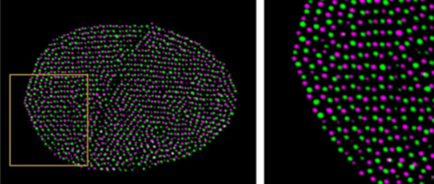
Crystalline 3D patterns of gold-polystyrene nanoparticles. Images captured via STEM tomography at the Molecular Foundry. (Credit: Berkeley Lab)
Using microscopes at the Molecular Foundry, a world-leading user facility in STEM tomography, the researchers first captured crystalline 3D patterns of the Au-PS nanoparticles.
On the hunt for more clues, Xu and Qian then deployed nuclear magnetic resonance spectroscopy experiments at UC Berkeley, where they discovered a tiny trace of polyolefin molecules from the centrifuge tube lining had somehow entered the mix. Polyolefins, which include polyethylene and polypropylene, are some of the most ubiquitous plastics in the world.
Qian repeated the experiment, adding more polyolefin to the Au-PS solution – and this time, they got bigger 3D PGNP crystals within minutes.
Xu was surprised. “I thought, ‘This shouldn’t be happening so fast,’” she recalled. “Crystals of nanoparticles usually take days to grow in the lab.”
A boon for industry: growing materials at the nanolevel
Subsequent experiments revealed that as the toluene solvent quickly evaporates at room temperature, the polyolefin additive helps the Au-PS nanoparticles form into 3D PGNP crystals, and to “grow into their favorite crystal structure,” said Qian.
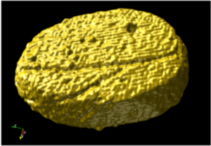
In another key experiment, the researchers designed a self-assembling 100-200-nanometer crystalline disc that looks like the base of a pyramid. From this stunning demonstration of mastery over matter at the nanolevel, the researchers learned that the size and shape of the 3D PGNP crystals are driven by the kinetic energy of the polyolefins as they precipitate in the solution.
Altogether, these findings “provide a model for showing how you can control the crystal structure at the single particle level,” Xu said, adding that their discovery is exciting because it provides new insight into how crystals form during the early stages of nucleation.
“And that’s challenging to do because it’s hard to make atoms sit next to each other,” Ercius said.
The new approach could grant researchers unprecedented control in fine-tuning electronic and optical devices at the nanolevel (billionths of a meter), Xu said. Such nanoparticle-scale precision, she added, could speed up production and eliminate errors in manufacturing.
Looking ahead, Qian would like to use their new technique to probe the toughness of different crystal structures – and perhaps even make a hexagonal crystal.
Xu plans to use their technique to grow bigger devices such as a transistor or perhaps 3D-print nanoparticles from a mix of materials.
“What can you do with different morphologies? We’ve shown that it’s possible to generate a single-component composite from a mineral and a polymer. It’s really exciting. Sometimes you just need to be in the right place at the right time,” Xu said.
Other co-authors on the paper include Alessandra da Silva and Wolfgang Theis at the University of Birmingham in the United Kingdom; Emmy Yu, an undergraduate student researcher in the Xu Group at UC Berkeley; and Christopher L. Anderson and Yi Liu at Berkeley Lab’s Molecular Foundry.
The Molecular Foundry is a DOE Office of Science nanoscience user facility at Berkeley Lab.
The work was supported by the DOE Office of Science.
###
Founded in 1931 on the belief that the biggest scientific challenges are best addressed by teams, Lawrence Berkeley National Laboratory and its scientists have been recognized with 14 Nobel Prizes. Today, Berkeley Lab researchers develop sustainable energy and environmental solutions, create useful new materials, advance the frontiers of computing, and probe the mysteries of life, matter, and the universe. Scientists from around the world rely on the Lab’s facilities for their own discovery science. Berkeley Lab is a multiprogram national laboratory, managed by the University of California for the U.S. Department of Energy’s Office of Science.
DOE’s Office of Science is the single largest supporter of basic research in the physical sciences in the United States, and is working to address some of the most pressing challenges of our time. For more information, please visit energy.gov/science.


