Artist’s illustration of hydrodynamical behavior from an interacting ensemble of quantum spin defects in diamond. (Credit: Norman Yao/Berkeley Lab)
– By Rachel Berkowitz
In 1998, researchers including Mark Kubinec of UC Berkeley performed one of the first simple quantum computations using individual molecules. They used pulses of radio waves to flip the spins of two nuclei in a molecule, with each spin’s “up” or “down” orientation storing information in the way that a “0” or “1” state stores information in a classical data bit. In those early days of quantum computers, the combined orientation of the two nuclei – that is, the molecule’s quantum state – could only be preserved for brief periods in specially tuned environments. In other words, the system quickly lost its coherence. Control over quantum coherence is the missing step to building scalable quantum computers.
Now, researchers are developing new pathways to create and protect quantum coherence. Doing so will enable exquisitely sensitive measurement and information processing devices that function at ambient or even extreme conditions. In 2018, Joel Moore, a senior faculty scientist at Lawrence Berkeley National Laboratory (Berkeley Lab) and professor at UC Berkeley, secured funds from the Department of Energy to create and lead an Energy Frontier Research Center (EFRC) – called the Center for Novel Pathways to Quantum Coherence in Materials (NPQC) – to further those efforts. “The EFRCs are an important tool for DOE to enable focused inter-institutional collaborations to make rapid progress on forefront science problems that are beyond the scope of individual investigators,” said Moore.
Through the NPQC, scientists from Berkeley Lab, UC Berkeley, UC Santa Barbara, Argonne National Laboratory, and Columbia University are leading the way to understand and manipulate coherence in a variety of solid-state systems. Their threefold approach focuses on developing novel platforms for quantum sensing; designing two-dimensional materials that host complex quantum states; and exploring ways to precisely control a material’s electronic and magnetic properties via quantum processes. The solution to these problems lies within the materials science community. Developing the ability to manipulate coherence in realistic environments requires in-depth understanding of materials that could provide alternate quantum bit (or “qubit”), sensing, or optical technologies.
Basic discoveries underlie further developments that will contribute to other DOE investments across the Office of Science. As the program enters its fourth year, several breakthroughs are laying the scientific groundwork for innovations in quantum information science.
More defects, more opportunities
Many of NPQC’s achievements thus far focus on quantum platforms that are based on specific flaws in a material’s structure called spin defects. A spin defect in the right crystal background can approach perfect quantum coherence, while possessing greatly improved robustness and functionality.
These imperfections can be used to make high-precision sensing platforms. Each spin defect responds to extremely subtle fluctuations in the environment; and coherent collections of defects can achieve unprecedented accuracy and precision. But understanding how coherence evolves in a system of many spins, where all the spins interact with one another, is daunting. To meet this challenge, NPQC researchers are turning to a common material that turns out to be ideal for quantum sensing: diamond.

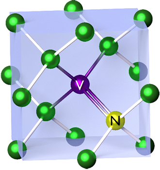
During diamond’s formation, replacement of a carbon atom (green) with a nitrogen atom (yellow, N) and omitting another to leave a vacancy (purple, V) creates a common defect that has well-defined spin properties. (Credit: NIST)
In nature, each carbon atom in a diamond’s crystal structure connects to four other carbon atoms. When one carbon atom is replaced by a different atom or omitted altogether, which commonly occurs as the diamond’s crystal structure forms, the resulting defect can sometimes behave like an atomic system that has a well-defined spin – an intrinsic form of angular momentum carried by electrons or other subatomic particles. Much like these particles, certain defects in diamond can have an orientation, or polarization, that is either “spin-up” or “spin-down.”
By engineering multiple different spin defects into a diamond lattice, Norman Yao, a faculty scientist at Berkeley Lab and an assistant professor of physics at UC Berkeley, and his colleagues created a 3D system with spins dispersed throughout the volume. Within that system, the researchers developed a way to probe the “motion” of spin polarization at tiny length scales.

Schematic depicting a central pocket of excess spin (turquoise shading) in a diamond cube, which then spread out much like dye in a liquid. (Credit: Berkeley Lab)
Using a combination of measurement techniques, the researchers found that spin moves around in the quantum mechanical system in almost the same way that dye moves in a liquid. Learning from dyes has turned out to be a successful path toward understanding quantum coherence, as recently published in the journal Nature. Not only does the emergent behavior of spin provide a powerful classical framework for understanding quantum dynamics, but the multi-defect system provides an experimental platform for exploring how coherence works as well. Moore, the NPQC director and a member of the team who has previously studied other kinds of quantum dynamics, described the NPQC platform as “a uniquely controllable example of the interplay between disorder, long-ranged dipolar interactions between spins, and quantum coherence.”
Those spin defects’ coherence times depend heavily on their immediate surroundings. Many NPQC breakthroughs have centered on creating and mapping the strain sensitivity in the structure surrounding individual defects in diamond and other materials. Doing so can reveal how best to engineer defects that have the longest possible coherence times in 3D and 2D materials. But exactly how might the changes imposed by forces on the material itself correlate to changes in the defect’s coherence?
To find out, NPQC researchers are developing a technique for creating deformed areas in a host crystal and measuring the strain. “If you think about atoms in a lattice in terms of a box spring, you get different results depending on how you push on them,” said Martin Holt, group leader in electron and X-ray microscopy at Argonne National Laboratory and a principal investigator with NPQC. Using the Advanced Photon Source and Center for Nanoscale Materials, both user facilities at Argonne National Laboratory, he and his colleagues offer a direct image of the deformed areas in a host crystal. Until now, a defect’s orientation in a sample has been mostly random. The images reveal which orientations are the most sensitive, providing a promising avenue for high-pressure quantum sensing.

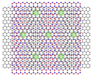
Scientists at Berkeley Lab and UC Berkeley unexpectedly discovered superconductivity in a triple layer of carbon sheets. (Credit: Feng Wang and Guorui Chen/Berkeley Lab)
“It’s really beautiful that you can take something like diamond and bring utility to it. Having something simple enough to understand the basic physics but that also can be manipulated enough to do complex physics is great,” said Holt.
Another goal for this research is the ability to transfer a quantum state, like that of a defect in diamond, coherently from one point to another using electrons. Work by NPQC scientists at Berkeley Lab and Argonne Lab studies special quantum wires that appear in atomically thin layers of some materials. Superconductivity was unexpectedly discovered in one such system, a triple layer of carbon sheets, by the group led by Feng Wang, a Berkeley Lab faculty senior scientist and UC Berkeley professor, and leader of NPQC’s effort in atomically thin materials. Of this work, published in Nature in 2019, Wang said, “The fact that the same materials can offer both protected one-dimensional conduction and superconductivity opens up some new possibilities for protecting and transferring quantum coherence.”
Toward useful devices
Multi-defect systems are not only important as fundamental science knowledge. They also have the potential to become transformative technologies. In novel two-dimensional materials that are paving the way for ultra-fast electronics and ultra-stable sensors, NPQC researchers investigate how spin defects may be used to control the material’s electronic and magnetic properties. Recent findings have offered some surprises.
“A fundamental understanding of nanoscale magnetic materials and their applications in spintronics has already led to an enormous transformation in magnetic storage and sensor devices. Exploiting quantum coherence in magnetic materials could be the next leap towards low-power electronics,” said Peter Fischer, senior scientist and division deputy in the Materials Sciences Division at Berkeley Lab.
A material’s magnetic properties depend entirely on the alignment of spins in adjacent atoms. Unlike the neatly aligned spins in a typical refrigerator magnet or the magnets used in classical data storage, antiferromagnets have adjacent spins that point in opposite directions and effectively cancel each other out. As a result, antiferromagnets don’t “act” magnetic and are extremely robust to external disturbances. Researchers have long sought ways to use them in spin-based electronics, where information is transported by spin instead of charge. Key to doing so is finding a way to manipulate spin orientation and maintain coherence.
![A team of researchers at Berkeley Lab and UC Berkeley have developed an antiferromagnetic switch for computer memory and processing applications. Credit: James Analytis/Berkeley Lab]](https://newscenter.lbl.gov/wp-content/uploads/2020/04/Fine-tuning-magnetic-spin-1063-300x300.png)
An exotic magnetic device could further miniaturize computing devices and personal electronics without loss of performance. Scale bar shown above is 10 micrometers (Credit: James Analytis/Berkeley Lab)
In 2019 NPQC researchers led by James Analytis, a faculty scientist at Berkeley Lab and associate professor of physics at UC Berkeley, with postdoc Eran Maniv, observed that applying a small, single pulse of electrical current to tiny flakes of an antiferromagnet caused the spins to rotate and “switch” their orientation. As a result, the material’s properties could be tuned extremely quickly and precisely. “Understanding the physics behind this will require more experimental observations and some theoretical modeling,” said Maniv. “New materials could help reveal how it works. This is the beginning of a new research field.”
Now, the researchers are working to pinpoint the exact mechanism that drives that switching in materials fabricated and characterized at the Molecular Foundry, a user facility at Berkeley Lab. Recent findings, published in Science Advances and Nature Physics, suggest that fine-tuning the defects in a layered material could provide a reliable means of controlling the spin pattern in new device platforms. “This is a remarkable example of how having many defects lets us stabilize a switchable magnetic structure,” said Moore, the NPQC leader.
Spinning new threads
In its next year of operation, NPQC will build on this year’s progress. Goals include exploring how multiple defects interact in two-dimensional materials and investigating new kinds of one-dimensional structures that could arise. These lower-dimensional structures could prove themselves as sensors for detecting other materials’ smallest-scale properties. Additionally, focusing on how electric currents can manipulate spin-derived magnetic properties will directly link fundamental science to applied technologies.
Rapid progress in these tasks requires the combination of techniques and expertise that can only be created within a large collaborative framework. “You don’t develop capabilities in isolation,” said Holt. “The NPQC provides the dynamic research environment that drives the science and harnesses what each lab or facility is doing.” The research center meanwhile provides a unique education at the frontiers of science including opportunities for developing the scientific workforce that will lead the future quantum industry.
The NPQC brings a new set of questions and goals to the study of the basic physics of quantum materials. Moore said, “Quantum mechanics governs the behavior of electrons in solids, and this behavior is the basis for much of the modern technology we take for granted. But we are now at the beginning of the second quantum revolution, where properties like coherence take center stage, and understanding how to enhance these properties opens a new set of questions about materials for us to answer.”
###
Founded in 1931 on the belief that the biggest scientific challenges are best addressed by teams, Lawrence Berkeley National Laboratory and its scientists have been recognized with 14 Nobel Prizes. Today, Berkeley Lab researchers develop sustainable energy and environmental solutions, create useful new materials, advance the frontiers of computing, and probe the mysteries of life, matter, and the universe. Scientists from around the world rely on the Lab’s facilities for their own discovery science. Berkeley Lab is a multiprogram national laboratory, managed by the University of California for the U.S. Department of Energy’s Office of Science.
DOE’s Office of Science is the single largest supporter of basic research in the physical sciences in the United States, and is working to address some of the most pressing challenges of our time. For more information, please visit energy.gov/science.
