
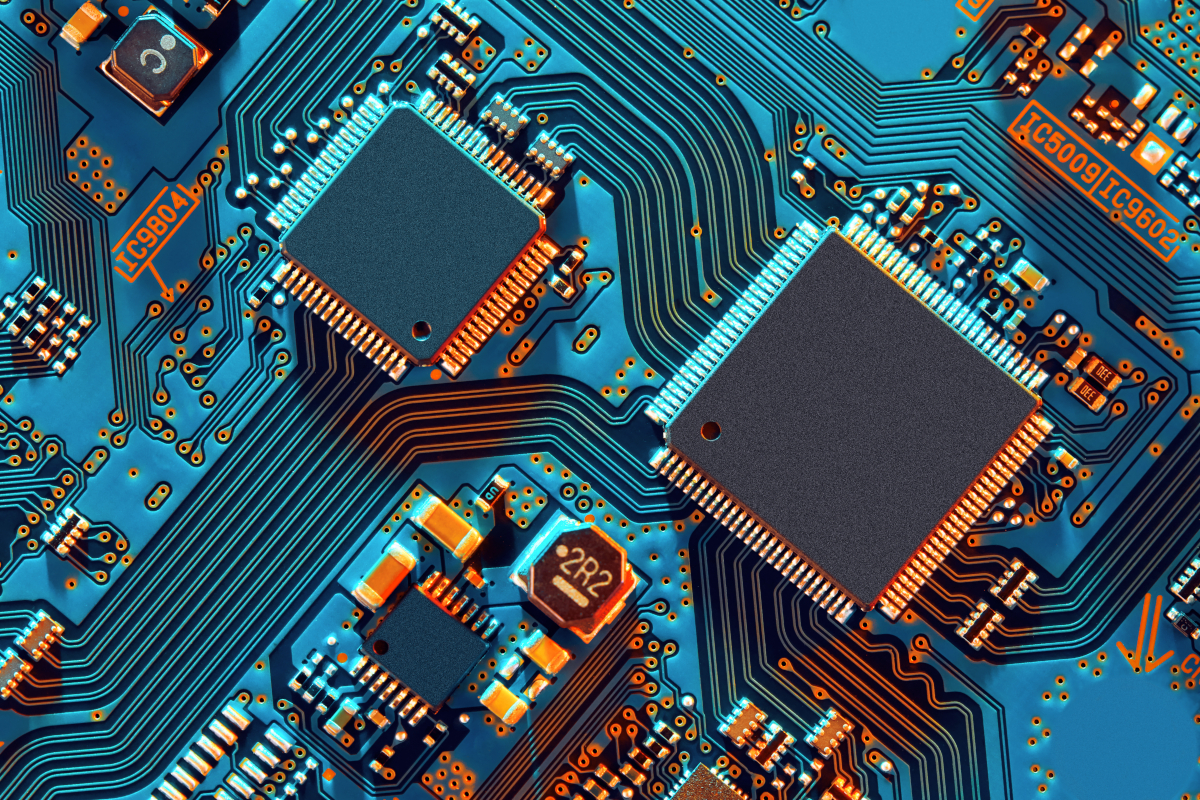
Computer chips on an electronic circuit board. (Credit: raigvi/Shutterstock)
Our laptops and smartphones are compact yet powerful because of silicon microelectronics, also known as microchips or chips, the tiny brains behind the digital brawn of almost every modern device.
But such modern convenience comes at a cost. By 2030, about 25% of the world’s energy – most of which is produced by burning carbon-rich fossil fuels – could be consumed by electronic devices if nothing is done to make them more energy efficient.
Silicon chips originate from a design known as CMOS, shorthand for complementary metal-oxide-semiconductor. As Moore’s Law first predicted in 1975, CMOS silicon chips are approaching limits in miniaturization and performance. For decades, scientists have been on the hunt for new electronic materials that go beyond the limits of Moore’s Law as well as the constraints of silicon CMOS chips.
Now, scientists Maurice Garcia-Sciveres and Ramamoorthy Ramesh at DOE’s Lawrence Berkeley National Laboratory (Berkeley Lab) are designing new microchips that could perform better – and require less energy – than silicon. Over the next three years, they will lead two of the 10 projects recently awarded nearly $54 million by the Department of Energy to increase energy efficiency in microelectronics design and production.
They discuss their projects in this Q&A.

Berkeley Lab scientists Maurice Garcia-Sciveres (left) and Ramamoorthy Ramesh are designing new microchips that could perform better – and require less energy – than silicon. (Courtesy of Garcia-Sciveres and Ramesh)
Q: Over the next 3 years, what do you hope to achieve? What is the significance of your work?
Garcia-Sciveres: Our project – the “Co-Design and Integration of Nano-Sensors on CMOS” – aims to improve performance by integrating tiny light sensors made with nanomaterials into a conventional CMOS (complementary metal-oxide-semiconductor) integrated circuit. (A nanomaterial is matter designed at an ultrasmall scale of a billionth of a meter.)
CMOS chips are made of silicon, but if you look at how much power silicon uses, it’s starting to be significant – and in a decade, silicon chips will be consuming a large fraction of our energy. For example, the computing needed to run a self-driving car consumes significant energy compared to the energy needed to run the car. We need to compute with less energy, or increase performance without more power, but you can’t do that with silicon chips because silicon has to run on a certain voltage – and those physical limitations are costing us.
In our project, nanomaterials such as carbon nanotubes – devices so small that they are invisible to the naked eye – would serve as light sensors. The nanosensors add new functionality to a CMOS chip, increasing performance.
Sensing is a good initial application, but when integrated into a chip, the carbon nanotubes could also serve as transistors or switches that process data. Integrating many carbon nanotubes into a silicon chip could lead to new kinds of electronic devices that are smaller and faster as well as more energy efficient than current technologies.
Ramesh: In our project, “Co-Design of Ultra-Low-Voltage Beyond CMOS Microelectronics,” we plan to explore new physical phenomena that will lead to significantly higher energy efficiency in computing. This is important because we believe that the next Moore’s Law is likely to be focused on the energy scale and not the length scale, since we are already at the limits of length scaling.
In around 2015, energy consumption from microelectronics was only about 4-5% of the world’s total primary energy. Primary energy typically means the chemical energy produced by a coal- or natural gas-based power plant. This typically has an efficiency of conversion to electricity of 35-40%.
Our increasing reliance on artificial intelligence, machine learning, and IoT – or the Internet of Things where everything is electronically connected, such as our traffic systems, emergency response systems, and renewable energy and electrical grid systems – will lead to an exponential increase of electronics from the systems perspective.
This means that by 2030, energy consumption from microelectronics is projected to be at least 25% of primary energy. Therefore, making electronics more energy efficient is a big deal.
For our project, we are asking, “What fundamental materials innovations could significantly scale back the energy consumption of microelectronics?” We’re looking at a totally different framework that explores new physics using a co-design approach, in which world-leading experts in materials physics, device and circuit design, fabrication and testing, and chip-level architecture are working in collaboration to carry out a holistic study of pathways to next-generation computing.
Q: What new applications will your work enable, and how will you demonstrate these new capabilities?
Garcia-Sciveres: Our work will demonstrate a single-photon imager that can measure the spectrum – the wavelength or energy – of every single photon or light particle it detects. This allows for hyperspectral imaging – that is, images where each pixel can be decomposed into many colors, providing much more information. Hyperspectral imaging benefits a broad range of science, from cosmology to biological imaging.
The Dark Energy Spectroscopic Experiment (DESI), an international science collaboration managed by Berkeley Lab, captures the spectra of distant galaxies, starting from images of the galaxies that were previously taken with other instruments. This added spectral information helps cosmologists understand how dark energy shaped the expansion of our universe. Had the original observations of the galaxies been made with a hyperspectral imager, spectral information would have been available to begin with.
Another growing application of hyperspectral imaging is the study of exoplanets. (Planets in our solar system orbit around the Sun. Planets that orbit around other stars are called exoplanets.)
But the sensors used for these types of observations work at temperatures less than 1 degree above absolute zero. Our device would work at more practical temperatures, perhaps even up to room temperature.
Hyperspectral imaging has many applications in medicine and biosciences, and many commercial instruments are available. However, these instruments, which are all much more complex and more expensive than a regular camera, either scan an object pixel by pixel or have complex arrangements of robotic fibers or filters. Moreover, these instruments do not have single-photon sensitivity. Our device would enable a simple camera that provides hyperspectral images with single-photon sensitivity.
Ramesh: Our team is designed to demonstrate the viability and power of our co-design platform, “Atoms to Architecture,” which is built upon two fundamental physical phenomena:
The first is a novel behavior in ferroelectric-based transistor architectures that provides a pathway to reduce the total energy consumed in a silicon-based microelectronics device. (A ferroelectric is a material with an electrical dipole – or a pair of positive and negative electrical charges – that is switchable with an electric field.) The second is the low-voltage electric field manipulation of electronic spin using a novel class of materials called multiferroics.
In 2014, we demonstrated a magneto-electric material that can convert charge into magnetic spin at 5 volts of applied voltage. Subsequent collaborative work with researchers at Intel showed how this could be used to create a new class of logic-in-memory devices, termed the MESO device, which uses spins to carry out logic operations.
For one of our projects within our program, we will use our magneto-electric material to explore multiferroic elements that will function at 100 millivolts, leading to a significant drop in energy consumption. (A millivolt is one thousandth of a volt.)
Our second project is exploring the fundamental physics of a capacitor device, in which a ferroelectric layer is overlaid on a conventional silicon transistor to enhance its energy efficiency through what’s known as the negative capacitance effect. Our design would enable a microelectronics device that carries out both memory and logic functions – This approach is radically different from the chips in our computers today, where one kind of chip performs the logic or processing of data, and another chip stores data.
The “Co-Design and Integration of Nano-Sensors on CMOS” project is a collaboration between researchers at Berkeley Lab, Sandia National Laboratory, and UC Berkeley. Co-principal investigators include Weilun Chao, Steve Holland, Mi-Young Im, Tevye Kuykendall, Francois Leonard, Yuan Mei, Andrew Nonaka, Katerina Papadopoulou, Greg Tikhomoirov, Archana Raja, Ricardo Ruiz, and Jackie Yao.
The “Co-Design of Ultra-Low-Voltage Beyond CMOS Microelectronics project” is a collaboration between researchers at Berkeley Lab and UC Berkeley. Co-principal investigators include Sinéad Griffin, Lane Martin, Lavanya Ramakrishnan, Sayeef Saluhuddin, Padraic Shafer, John Shalf, Dilip Vasudevan, and Jackie Yao.
###
Founded in 1931 on the belief that the biggest scientific challenges are best addressed by teams, Lawrence Berkeley National Laboratory and its scientists have been recognized with 14 Nobel Prizes. Today, Berkeley Lab researchers develop sustainable energy and environmental solutions, create useful new materials, advance the frontiers of computing, and probe the mysteries of life, matter, and the universe. Scientists from around the world rely on the Lab’s facilities for their own discovery science. Berkeley Lab is a multiprogram national laboratory, managed by the University of California for the U.S. Department of Energy’s Office of Science.
DOE’s Office of Science is the single largest supporter of basic research in the physical sciences in the United States, and is working to address some of the most pressing challenges of our time. For more information, please visit energy.gov/science.