Scientific Contacts: Kai Vetter, Lucian Mihailescu

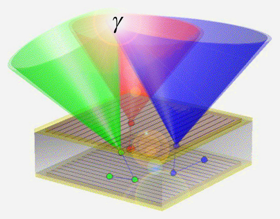
How a gamma-ray camera makes an image: when any three gamma-ray photons are absorbed in a segmented germanium detector, their source can be found by calculating all possible directions, mapped as the surfaces of cones, from which each photon may have arrived. The source (Greek gamma) lies at the point where all three cones intersect.
In 2008 Berkeley Lab’s Nuclear Science Division (NSD) launched the Applied Nuclear Physics program, headed by NSD’s Kai Vetter upon his return to Berkeley after six years with Lawrence Livermore National Laboratory. One of the goals of Applied Nuclear Physics is to take experimental principles and equipment created for basic research and develop them into tools that can address practical needs like cancer therapy and homeland security.
“Pure science and practical applications push each other,” says Vetter, who is also a professor in residence in UC Berkeley’s Department of Nuclear Engineering. “Adapting laboratory devices to real-world uses gives us many opportunities to demonstrate new techniques, which often turn out to benefit science as well.”
Among the prime examples of instruments with this kind of versatility are gamma-ray detectors. Two such adaptations have recently earned substantial support from DOE’s Office of Nuclear Physics. One, funded directly by DOE, will improve the scope and resolution of radiation spectrographs. The other, funded via the American Recovery and Reinvestment Act (ARRA), will develop techniques for three-dimensional imaging of gamma-ray sources.
Gamma rays and 3-D images
The 3-D imaging project is a three-year, $1 million-plus program whose principal investigator is NSD’s Lucian Mihailescu. Mihailescu became interested in making images with gamma rays when he was a graduate student in Germany.
“My ambition really took off when I moved to the U.S. and went to work at Livermore,” Mihailescu says. “There they were interested in new ideas and applications, not only in predetermined research programs.”
At Livermore Mihailescu worked with Vetter, whose degrees are also from German universities, on a scheme to develop a Compton imager for the Department of Homeland Security—a “camera” that uses high-energy gamma rays, instead of lower-energy x-rays or visible light, to see through intervening matter and detect illicit radioactive sources. In its first iteration, the imager had to be carried around on a truck.
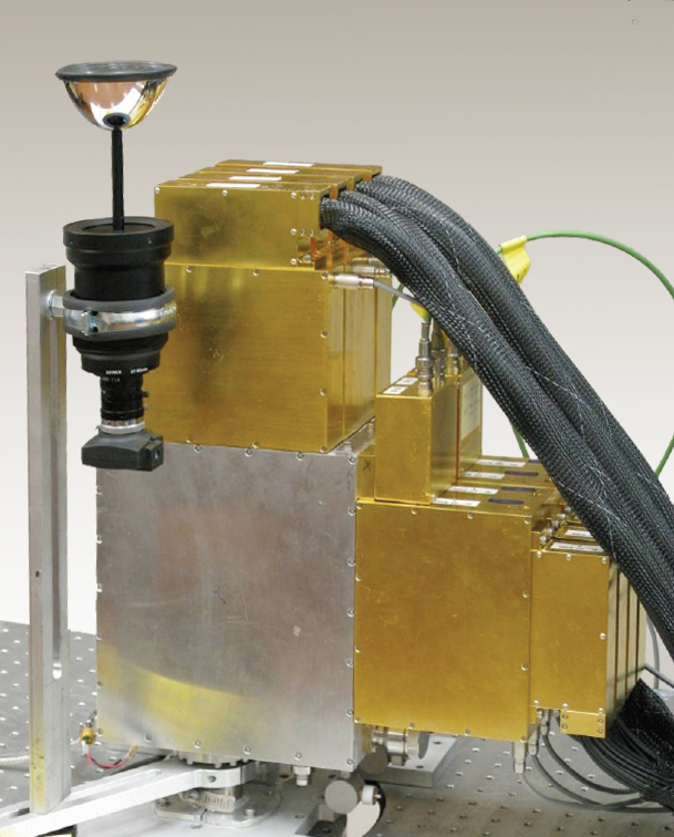
Berkeley Lab’s descendant of this imager is called the Compact Compton Imager 2 (CCI-2) and fits on a cart, although Mihailescu says “it still weighs a ton.” The ARRA grant is intended to help Mihailescu and Vetter refine a truly compact imager, working with colleagues including I-Yang Lee, who heads the GRETINA gamma-ray tracking collaboration. While it will be useful for security applications and also for basic science, the principal task of the new imager will be to improve the reliability and practicality of cancer therapy using heavy-ion beams.

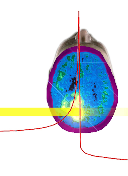
PET scans take too long to give a picture of whether an ion beam accurately hits its target. Gamma rays are emitted instantly when the beam interacts with tissue and could indicate the precise location and dose while there’s still time to adjust the treatment.
“DOE has a long interest in cancer therapy with protons and heavy ion beams because of the huge advantage over x-ray therapy,” says Vetter. “An ion beam can penetrate deep and deposit most of its energy right in the tumor, with minimal damage to surrounding tissue. But there’s a serious drawback. At present there’s no way to get a quick measure of the actual dose or how it’s distributed.”
Ideally, one should be able to make images during treatment, showing exactly where the ion beam is depositing its energy in the tumor. Imaging methods exist, but they take too long: a common therapy uses carbon ions, which react with nuclei in the tissue to create radioactive carbon-11. When carbon-11 decays, it emits positrons and so can be detected by positron-emission tomography, or PET scans.
But carbon-11’s half-life is more than 20 minutes, while the cancer treatment lasts only a few minutes. To collect enough data for an accurate dose measure and to find out where the beam actually ends up takes at least half an hour—much too late to obtain an accurate picture of the beam before the activity is diffused or adjust the treatment while underway … or stop it if necessary.
The ion beam excites oxygen and nitrogen as well as carbon when it encounters tissue, and all these excited nuclei instantly emit gamma rays. Here’s where the Compton gamma-ray imager comes in.
Playing billiards with light
When photons—particles of light (including gamma rays)—encounter matter, those of lower energy can transfer that energy to electrons and knock them right out of atoms; Einstein described this photoelectric effect in 1905. Higher-energy photons like gamma rays may transfer only part of their energy: like a collision of billiard balls, the electron rebounds in one direction and the reduced-energy photon scatters in another. Often a gamma ray does both, scattering off of one or more electrons before knocking one free and being absorbed. This is Compton scattering, named after physicist Arthur Holly Compton, who proposed it in 1923.

The Compact Compton Imager-2 with its coolant connectors and electronics must be transported on a cart. Research will provide better electronics and software, for higher accuracy in a smaller package.
For detecting gamma rays, germanium crystals cooled to the temperature of liquid nitrogen (minus 196 degrees Celsius, or 321 degrees Fahrenheit below zero) are particularly good. Gamma rays can penetrate germanium crystals deeply before the material absorbs them, and dividing the faces of a flat crystal into strips allows each event to be pinpointed on a grid.
CCI-2 uses a sandwich of two double-sided germanium detectors and two silicon detectors. By distinguishing a series of events along the path of each scattered gamma-ray photon, the energy, momentum, and angle of the original gamma ray can be calculated; by combining information from enough photons, an image of the source that emitted the gamma rays can be constructed.
“The trick is to record all the interactions,” says Mihailescu. “The basic idea was proposed as long ago as the 1970s, but it’s only recently that commercial semiconductor crystals have gotten sensitive enough, and computers powerful enough, to collect and keep track of everything. One of our tasks is to upgrade our electronics so we can improve the count-rate from 3,000 gamma-ray hits per second to potentially a million per second.”
Even at its present slow count-rate, CCI-2 can collect and process enough data to construct a 3-D movie of a line source of cesium-137 inside a thin pipe in a room, or a picture that distinguishes two small spheres of tin-113 placed close together. Improved electronics and algorithms, based on those used for the big research detector, GRETINA, will lead to higher resolution and faster response.
An animated version of an actual classroom demonstration, showing the CCI-2’s ability to detect and image hidden radioactive sources at a distance in three dimensions.
“The data used to construct these images allows them to be superposed on visible or x-ray images and viewed from any angle within 360 degrees, ideal for imaging during radiation therapy,” Mihailescu says. “And by adding time discrimination, someday we’ll be able to correlate the sources with moving objects.”
The next iteration of the Compton imager will be tested with GRETINA, using beams from the 88-Inch Cyclotron. The results will contribute to basic science studies and may be especially pertinent to radioactive-beam facilities like those recently approved by DOE for the new Facility for Rare Isotope Beams (FRIB) to be built at Michigan State University.
“Imaging will help distinguish the radiation of interest in the experiment from the radioactive background caused by the beams,” Vetter says, “and it will enable new concepts in measuring lifetimes of nuclear states that would be almost inaccessible by other means.”
The improved gamma-ray imager will contribute to nuclear security techniques such as neutron activation and nuclear resonance fluorescence. In an age when nuclear materials in the wrong hands are a greater threat than nuclear war, when assured destruction is no deterrent, critical components in guarding against terrorist attack are detection, proliferation prevention, and safeguards.
But most important, the improved Compact Compton Imager will enable greater precision at lower risk for one of the most promising methods of radiation cancer therapy—and, eventually perhaps, many more biomedical applications.
Detectors, from surfaces to fields
Berkeley Lab has a long history developing semiconductor detectors for radiation spectrometry and imaging. Improving the efficiency of these detector systems is the goal of the second major project that DOE is funding in NSD’s Applied Nuclear Physics program. The effort, led by Vetter and Mark Amman of the Engineering Division, focuses on improving fabrication processes and shaping the electric fields that collect signals from gamma rays caught by detectors made of high-purity germanium.
“Recently it has been possible to realize a concept first proposed by Berkeley Lab’s Paul Luke 20 years ago, with the result that the ‘application space’ of these detectors is still expanding,” says Vetter. “We want to expand it further. We want to reduce electronic noise and enhance charge collection properties in a variety of semiconductor detectors, to make them more efficient and capable of higher resolution.”
Depending on what it’s used for, a typical semiconductor detector may be eight centimeters in diameter (3.15 inches) and two to eight centimeters thick. Its surfaces are typically divided into segments by strips of metal that act as contacts to collect the charge carriers—electrons and holes—released when a gamma ray photon is absorbed.
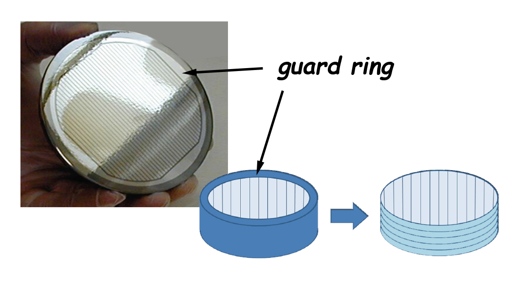
“The problem is the noncontact surfaces, which degrade the charge-collection process and cause leakage current,” Vetter says. “Those include the areas between the metal strips and also the sides of the detectors. To prevent leakage, the edges are often shielded by a thick guard ring, which may be of metal or other material, which severely cuts into the area of the detector.”
For better radiation detection, the researchers first need to maximize the usable surface area. To get rid of guard rings it will be necessary to find better ways to isolate the bare surfaces of the semiconductors from their surroundings. Part of the job can be done by segmenting the sides of the detector with metal contact strips, just as the planar surfaces are segmented. But real improvement will require better surface treatments and fabrication processes.

New surface treatments could eliminate the need for guard rings, and efficiency can be increased by shaped electric fields, achieved by segmenting the sides of the detector or trading the contact strips on one face for a point-contact electrode.
Another major effort will be to shape the electric fields in the detector, making the collection of charges resulting from radiation absorption more efficient. This would reduce electronic noise and improve resolution and increase the ability of the detector to localize events inside its bulk. The researchers will experiment with complex electrode schemes, including segmenting the detector’s edges. On the planar surfaces, contact strips can divide the entire area into segments, or a point contact can collect all the charges at a single electrode.
“As yet we don’t understand the physics of the detector surfaces well enough,” Vetter says. “Luckily Berkeley Lab’s Semiconductor Laboratory and UC Berkeley’s Gamma-Ray Imaging Laboratory will give us the ability to explore a range of processes and treatments and evaluate the results.”
More sensitive radiation detectors will benefit many practical applications, including the ability to identify quantities and kinds of radioactive materials for nuclear safeguards or to monitor nuclear reactors. They will also benefit the most basic science: the search for the theoretical constituents of dark matter and for certain kinds of radioactive decay (neutrinoless double beta decay) that would indicate that neutrinos are their own antiparticles, perhaps opening new ways to measure the mass of these elusive particles.
The new grants to NSD’s Applied Nuclear Physics program will result in the hiring of two postdoctoral researchers and will support two part-time UC graduate student researchers. The projects will involve not only Vetter, Mihailescu, Lee, and Amman but other NSD and Engineering staff scientists as well. The projects will be done in close cooperation with UC Berkeley’s Department of Nuclear Engineering.
Additional information
Wikipedia’s article on particle therapy, including heavy-ion therapy
Wikipedia’s article on Compton scattering
More on Berkeley Lab’s contributions to the Facility for Rare Isotope Beams (FRIB)
More on the genesis of the Compact Compton Imager at Lawrence Livermore Lab
More on semiconductor radiation detectors, including germanium detectors
An update on the GRETINA detector will soon appear on the News Center.