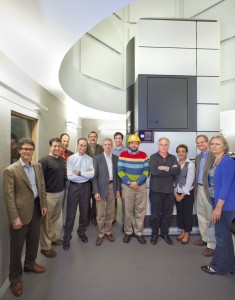
The project management team behind the design and construction of TEAM, the world’s most powerful electron microscope and the first successful multi-institutional collaborative development project in the 80-year history of electron microscopy, has won a prestigious “Secretary of Energy’s Excellence in Acquisition Award.” This award is given by the U.S. Department of Energy (DOE) to management teams that have demonstrated “exceptional results in completing a project within cost and schedule.”

The Energy Secretary’s Excellence Award for exceptional project performance now decorates TEAM I, the world’s best electron microscope. A celebration included many of the TEAM project team including project manager Peter Denes (in yellow hard hat) and project director Uli Dahmen to his immediate left. (Photo by Roy Kaltschmidt, Berkeley Lab Public Affairs)
“TEAM” stands for Transmission Electron Aberration-corrected Microscope, and the project involved two separate instruments. The first instrument, dubbed TEAM 0.5, was installed at the start of 2008. It delivered a resolution of 0.5 angstroms, which is less than the diameter of a single hydrogen atom, and provided a unique ability to correct for the image-degrading phenomenon known as spherical aberration. In September, 2009, a second even better instrument – TEAM I – was installed. In addition to 0.5 angstrom resolution and spherical aberration correction, TEAM I is also able to correct for chromatic aberration, a problem that arises when a lens refracts light or electrons of different wavelengths at different angles. Chromatic aberration has never before been accomplished in an electron microscope.
The TEAM Project was a collaboration led by DOE’s Lawrence Berkeley National Laboratory (Berkeley Lab) and including DOE’s Argonne and Oak Ridge National Laboratories, the Frederick Seitz Materials Laboratory of the University of Illinois, and two private companies specializing in electron microscopy, the FEI Company headquartered in Portland, Oregon which built the TEAM microscopes, and CEOS of Heidelberg, Germany which developed the new aberration correctors. The project began in June, 2004 and was completed at a cost of $27.1 million.
“TEAM was delivered on time and on budget, and reached its signature technical goal of 0.5 angstrom spatial resolution two years ahead of schedule,” said Peter Denes, acting director of Berkeley Lab’s Engineering Division, who served as the TEAM project manager. “Through careful planning, with a staged deliverable, the TEAM project was able to begin producing breakthrough scientific results more than a year before the end of the project.”
The TEAM microscopes are housed at the National Center for Electron Microscopy (NCEM), a DOE national user facility located at Berkeley Lab. NCEM is considered one of the world’s premier centers for electron microscopy and microcharacterization. It is directed by Ulrich Dahmen, who served as director of the TEAM collaborative project. Kathy Johnescu, of DOE’s Berkeley Site Office, served as TEAM’s Federal Project Director.
“It is particularly rewarding to see that the first project ever attempted by the microscopy community receive such a recognition,” Dahmen said. “For microscopists it’s like winning the gold medal the first time your team enters a race. The award gives a lot of credibility to the electron microscopy community and opens the door to future projects that have previously been thought to be out of range.”
The spectacular resolution and unique ability to correct for aberrations in combination with ultra-stable electronics and extremely bright electron source make the TEAM microscopes ideal for the study of how atoms combine to form materials, how materials grow, and how they respond to a variety of external factors. Already TEAM 0.5 has been used to produce a movie that shows in real-time carbon atoms repositioning themselves around the edge of a hole in a graphene sheet, and the first ever direct observations in real-time of the growth of single nanocrystals in solution.
In addition to developing the world’s best microscopes, TEAM project members also developed a novel sample positioning stage, which won an R&D 100 Award in 2009, considered the equivalent of an Oscar for inventions, as well as a new kind of high speed and high sensitivity electron detector.
“As a DOE Facilities for the Future of Science project, TEAM had vision and visibility far beyond its comparatively modest cost,” said Denes. “The success of the TEAM project has inspired similar projects in Europe and Japan.”
Berkeley Lab is a U.S. Department of Energy national laboratory located in Berkeley, California. It conducts unclassified scientific research for DOE’s Office of Science and is managed by the University of California. Visit our Website at www.lbl.gov/
Additional Information
For more information on the National Center for Electron Microscopy visit the Website at http://ncem.lbl.gov/