Contact: Aditi Risbud, (510)486-4861, [email protected]
Scientists at Berkeley Lab and the Institute for Microelectronics and Microsystems-CNR in Naples, Italy have experimentally demonstrated-for the first time-the concept of optical antimatter, in which light travels through a material without being distorted. By engineering a material that focuses light through its internal structure, a beam of light can enter and exit unperturbed after traveling through millimeters of material.

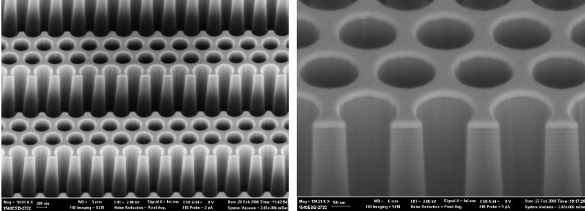
Berkeley Lab scientists have designed a novel device that demonstrates the concept of optical antimatter, in which light travels millimeter distances through matter without distortion. The electron microscope image in (a) shows the device’s alternating of space and silicon photonic crystalline material with air holes. The image (b) is a magnified version.
For years, optics researchers have struggled to bypass the diffraction limit, a physical law that restricts imaging resolution to about one-half the wavelength of light used to make the image. If a material with a negative index of refraction-a property describing how light bends as it enters or exits a material-could be designed, this diffraction hurdle could be lowered. Such a material could also behave as a ‘superlens,’ useful in imaging objects with detail finer than allowed by the diffraction limit.
Despite the intriguing possibilities posed by a substance with a negative index of refraction, this property is inaccessible through naturally occurring (positive index) materials. In the mid-1990s, English theoretical physicist Sir John Pendry proposed a clever ‘sleight of light’ by using so-called metamaterials-engineered materials whose underlying structure can alter the overall response to electrical and magnetic fields. Inspired by Pendry’s proposal, scientists have made progress in scaling metamaterials from microwave to infrared wavelengths, while illuminating the nuances of light’s speed and direction of motion in these engineered structures.
“We’ve shown a completely new way to control and manipulate light, using a silicon photonic crystal as a real metamaterial-and it works,” said Stefano Cabrini, Facility Director of the Nanofabrication Facility in the Molecular Foundry, a U.S. Department of Energy User Facility located at Berkeley Lab that provides support to nanoscience researchers around the world. “Our findings will open up an easier way to make and use structures that have a ‘superlens’ effect.”

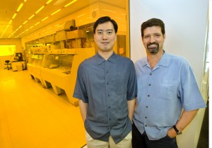
Berkeley Lab researchers Allan Chang (left) and Stefano Cabrini at The Molecular Foundry were part of an international collaboration that provided the first experimental evidence for optical antimatter. The device they created by alternating layers of air and a silicon photonic crystal containing air holes can serve as a superlens.
Through the Molecular Foundry user program, Cabrini and postdoctoral researcher Allan Chang collaborated with Vito Mocella, a theoretical scientist at the Institute of Microelectronics and Microsystems-CNR in Naples, Italy to fabricate a two by two millimeter device consisting of alternating layers of air and a silicon-based photonic crystal containing air holes. Using high-precision nanofabrication processes, the team designed the spacing and thicknesses of each layer to behave like the metamaterial Pendry had envisioned. This device was then used to focus a beam of near-infrared light, essentially annihilating two millimeters of space.
“Now that we have a prototype to demonstrate the concept, our next step will be to find the geometry and material that will work for visible light,” said Cabrini.
Along with the possibilities in imaging, the researchers’ findings could also be used to develop hybrid negative- and positive-index materials, Cabrini added, which may lead to novel devices and systems unachievable through either material alone.
“Self-collimation of light over millimeter-scale distance in a quasi-zero-average-index metamaterial,” by Vito Mocella, Stefano Cabrini, Allan S.P. Chang, P. Dardano, L. Moretti, I. Rendina, Deirdre Olynick, Bruce Harteneck and Scott Dhuey, appears in Physical Review Letters and is available in Physical Review Letters online.
Portions of this work were supported by the Office of Science, Office of Basic Energy Sciences of the DOE under Contract No. DE-AC0205CH11231.
The Molecular Foundry is one of the five DOE Nanoscale Science Research Centers (NSRCs), premier national user facilities for interdisciplinary research at the nanoscale. Together the NSRCs comprise a suite of complementary facilities that provide researchers with state-of-the-art capabilities to fabricate, process, characterize and model nanoscale materials, and constitute the largest infrastructure investment of the National Nanotechnology Initiative. The NSRCs are located at DOE’s Argonne, Brookhaven, Lawrence Berkeley, Oak Ridge and Sandia and Los Alamos National Laboratories. For more information about the DOE NSRCs, please visit http://nano.energy.gov.
Berkeley Lab is a U.S. Department of Energy national laboratory located in Berkeley, California. It conducts unclassified scientific research and is managed by the University of California. Visit our website at http://www.lbl.gov.
Additional Information
For more information about The Molecular Foundry and its user programs visit the Website at http://foundry.lbl.gov/