
Berkeley Lab researchers are using the science of the very small to help solve big challenges. That’s because, at the nanoscale—the scale of molecules and proteins—new and exciting properties emerge that can possibly be put to use.
Here are five projects, now underway and recently highlighted in the News Center, which promise big results from the smallest of building blocks:
1. A DIY paint-on coating for energy efficient windows
This “cool” DIY retrofit tech could improve the energy efficiency of windows and save money. Researchers are developing a polymer-based heat-reflective coating that makes use of the unusual molecular architecture of a polymer.
It has the potential to be painted on windows at one-tenth the cost of current retrofit approaches. Window films on the market today reflect infrared solar energy back to the sky while allowing visible light to pass through, but a professional contractor is needed to install them. A low-cost option could significantly expand adoption and result in potential annual energy savings equivalent to taking 5 million cars off the road.
2. Nanowires that move data at light speed
Researchers have found a new way to produce nanoscale wires that can serve as tiny, tunable lasers. The excellent performance of these tiny lasers is promising for the field of optoelectronics, which is focused on combining electronics and light to transmit data, among other applications. Miniaturizing lasers to the nanoscale could further revolutionize computing, bringing light-speed data transmission to desktop, and ultimately, handheld computing devices.
3. Nano sponges that fight climate change
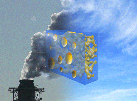
Scientists are developing nano sponges that could capture carbon from power plants before it enters the atmosphere. Initial tests show the hybrid membrane, composed of nano-sized cages (called metal-organic frameworks) and a polymer, is eight times more carbon dioxide permeable than membranes composed only of the polymer.
Boosting carbon dioxide permeability is a big goal in efforts to develop carbon capture materials that are energy efficient and cost competitive. Watch this video for more on this technology.
4. Custom-made chemical factories
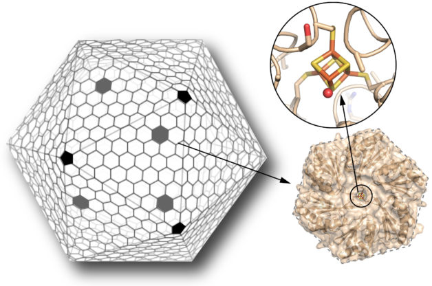
Scientists have recently reengineered a building block of a nanocompartment that occurs naturally in bacteria, greatly expanding the potential of nanocompartments to serve as custom-made chemical factories. Researchers hope to tailor this new use to produce high-value chemical products, such as medicines, on demand
The sturdy nanocompartments are formed by hundreds of copies of just three different types of proteins. Their natural counterparts, known as bacterial microcompartments, encase a wide variety of enzymes that carry out highly specialized chemistry in bacteria.
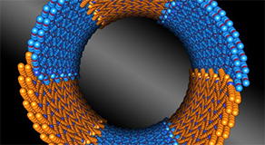
5. Nanotubes that assemble themselves
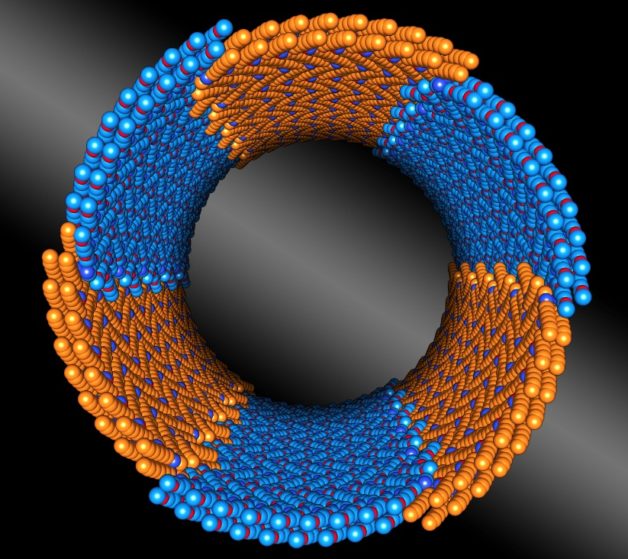
Researchers have discovered a family of nature-inspired polymers that, when placed in water, spontaneously assemble into hollow crystalline nanotubes. What’s more, the nanotubes can be tuned to all have the same diameter of between five and ten nanometers.
Controlling the diameter of nanotubes, and the chemical groups exposed in their interior, enables scientists to control what goes through. Nanotubes have the potential to be incredibly useful, from delivering cancer-fighting drugs inside cells to desalinating seawater.
The Science of Small Revealed Using a Penny
Just how small can nanoscience get? Here’s a great example using an American penny from the Molecular Foundry.
In this video, the letters that spell Molecular Foundry were written with a beam of electrons fired at the surface. The smallest feature is 20 nanometers, or roughly 100 atoms. As the video zooms out, you lose sight of Molecular Foundry and see the Berkeley Lab logo, which was written with a beam of charged gallium atoms. As you continue to zoom out, you see an 18 hour timelapse of Abraham Lincoln’s face, again written with gallium atoms. Finally, all of this is done within the Lincoln Memorial side of the penny as it is removed from the focused ion beam.
Photolithography, which literally means writing with light, is the foundation for most top-down fabrication of things like microprocessors. However, because of something called the diffraction limit, photolithography is limited to devices that have features no smaller than the wavelength of the light used, often in the 100s of nanometers. As a result, things smaller than light like atoms and electrons must be used.