Scientists have demonstrated a new material that conducts heat 150% more efficiently than conventional materials used in advanced chip technologies.
The device – an ultrathin silicon nanowire – could enable smaller, faster microelectronics with a heat-transfer-efficiency that surpasses current technologies. Electronic devices powered by microchips that efficiently dissipate heat would in turn consume less energy – an improvement that could help mitigate the consumption of energy produced by burning carbon-rich fossil fuels that have contributed to global warming.
“By overcoming silicon’s natural limitations in its capacity to conduct heat, our discovery tackles a hurdle in microchip engineering,” said Junqiao Wu, the scientist who led the Physical Review Letters study reporting the new device. Wu is a faculty scientist in the Materials Sciences Division and professor of materials science and engineering at UC Berkeley.
Heat’s slow flow through silicon
Our electronics are relatively affordable because silicon – the material of choice for computer chips – is cheap and abundant. But although silicon is a good conductor of electricity, it is not a good conductor of heat when it is reduced to very small sizes – and when it comes to fast computing, that presents a big problem for tiny microchips.
Within each microchip resides tens of billions of silicon transistors that direct the flow of electrons in and out of memory cells, encoding bits of data as ones and zeroes, the binary language of computers. Electrical currents run between these hard-working transistors, and these currents inevitably generate heat.
Heat naturally flows from a hot object to a cool object. But heat flow gets tricky in silicon.
In its natural form, silicon is made up of three different isotopes – forms of a chemical element containing an equal number of protons but different number of neutrons (hence different mass) in their nuclei.
About 92% of silicon consists of the isotope silicon-28, which has 14 protons and 14 neutrons; around 5% is silicon-29, weighing in at 14 protons and 15 neutrons; and just 3% is silicon-30, a relative heavyweight with 14 protons and 16 neutrons, explained co-author Joel Ager, who holds titles of senior scientist in Berkeley Lab’s Materials Sciences Division and adjunct professor of materials science and engineering at UC Berkeley.
As phonons, the waves of atomic vibration that carry heat, wind their way through silicon’s crystalline structure, their direction changes when they bump into silicon-29 or silicon-30, whose different atomic masses “confuse” the phonons, slowing them down.
“The phonons eventually get the idea and find their way to the cold end to cool the silicon material,” but this indirect path allows waste heat to build up, which in turn slows your computer down, too, Ager said.
A big step toward faster, denser microelectronics
For many decades, researchers theorized that chips made of pure silicon-28 would overcome silicon’s thermal conductivity limit, and therefore improve the processing speeds of smaller, denser microelectronics.
But purifying silicon down to a single isotope requires intense levels of energy which few facilities can supply – and even fewer specialize in manufacturing market-ready isotopes, Ager said.
Fortunately, an international project from the early 2000s enabled Ager and leading semiconductor materials expert Eugene Haller to procure silicon tetrafluoride gas – the starting material for isotopically purified silicon – from a former Soviet-era isotope manufacturing plant. (Haller founded Berkeley Lab’s DOE-funded Electronic Materials Program in 1984, and was a senior faculty scientist in Berkeley Lab’s Materials Sciences Division and a professor of materials science and mineral engineering at UC Berkeley. He died in 2018.)
This led to a series of pioneering experiments, including a 2006 study published in Nature, whereby Ager and Haller fashioned silicon-28 into single crystals, which they used to demonstrate quantum memory storing information as quantum bits or qubits, units of data stored simultaneously as a one and a zero in an electron’s spin.
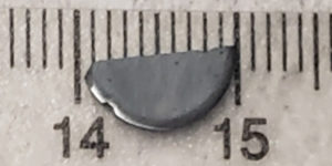
Optical microscopy image of a 99.92% silicon-28 crystal. Berkeley Lab scientist Junqiao Wu and his team used the 1 millimeter crystal to produce nanowires with a diameter of just 90 nanometers (billionths of a meter). (Credit: Junqiao Wu/Berkeley Lab)
Subsequently, semiconducting thin films and single crystals made with Ager’s and Haller’s silicon isotope material were shown to have a 10% higher thermal conductivity than natural silicon – an improvement, but from the computer industry’s point of view, probably not enough to justify spending a thousand times more money to build a computer from isotopically pure silicon, Ager said.
But Ager knew that the silicon isotope materials were of scientific importance beyond quantum computing. So he kept what remained in a safe place at Berkeley Lab, just in case other scientists might need it, because few people have the resources to make or even purchase isotopically pure silicon, he reasoned.
A path toward cooler tech with silicon-28
About three years ago, Wu and his graduate student Penghong Ci were trying to come up with new ways to improve the heat transfer rate in silicon chips.
One strategy to make more efficient transistors involves using a type of nanowire called a Gate-All-Around Field Effect Transistor. In these devices, silicon nanowires are stacked to conduct electricity, and heat is generated simultaneously, Wu explained. “And if the heat generated is not extracted out quickly, the device would stop working, akin to a fire alarm blaring in a tall building without an evacuation map,” he said.
But heat transport is even worse in silicon nanowires, because their rough surfaces – scars from chemical processing – scatter or “confuse” the phonons even more, he explained.
Optical microscopy image of a microdevice consisting of two suspended pads bridged by a silicon nanowire. (Credit: Junqiao Wu/Berkeley Lab)
“And then one day we wondered, ‘What would happen if we made a nanowire from isotopically pure silicon-28?’” Wu said.
Silicon isotopes are not something one can easily buy on the open market, and word had it that Ager still had some silicon isotope crystals in storage at Berkeley Lab – not a lot, but still enough to share “if someone has a great idea about how to use it,” Ager said. “And Junqiao’s new study was such a case.”
A surprising big reveal with nano tests
“We’re really fortunate that Joel happened to have the isotopically enriched silicon material ready to use for the study,” Wu said.
Using Ager’s silicon isotope materials, the Wu team tested the thermal conductivity in bulk 1-millimeter-size silicon-28 crystals versus natural silicon – and again, their experiment confirmed what Ager and his collaborators discovered years ago – that bulk silicon-28 conducts heat only 10% better than natural silicon.
Now for the nano test. Using a technique called electroless etching, Ci made natural silicon and silicon-28 nanowires just 90 nanometers (billionths of a meter) in diameter – about a thousand times thinner than a single strand of human hair.
To measure the thermal conductivity, Ci suspended each nanowire between two microheater pads outfitted with platinum electrodes and thermometers, and then applied an electrical current to the electrode to generate heat on one pad that flows to the other pad via the nanowire.
“We expected to see only an incremental benefit – something like 20% – of using isotopically pure material for nanowire heat conduction,” Wu said.
But Ci’s measurements astonished them all. The Si-28 nanowires conducted heat not 10% or even 20%, but 150% better than natural silicon nanowires with the same diameter and surface roughness.
This defied everything that they had expected to see, Wu said. A nanowire’s rough surface typically slows phonons down. So what was going on?
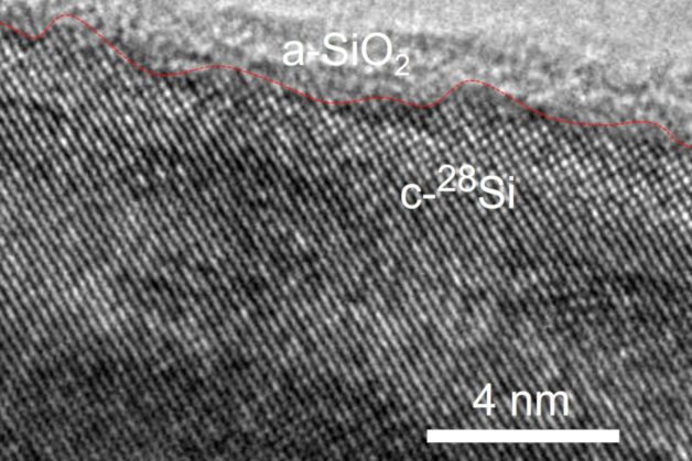
High-resolution TEM (transmission electron microscopy) images of the material captured by Matthew R. Jones and Muhua Sun at Rice University uncovered the first clue: a glass-like layer of silicon dioxide on the silicon-28 nanowire surface.
Computational simulation experiments at the University of Massachusetts Amherst led by Zlatan Aksamija, a leading expert on the thermal conductivity of nanowires, revealed that the absence of isotope “defects” – silicon-29 and silicon-30 – prevented phonons from escaping to the surface, where the silicon dioxide layer would drastically slow down the phonons. This in turn kept phonons on track along the direction of heat flow – and therefore less “confused” – inside the silicon-28 nanowire’s “core.” (Aksamija is currently an associate professor of materials science and engineering at the University of Utah.)
“This was really unexpected. To discover that two separate phonon-blocking mechanisms – the surface versus the isotopes, which were previously believed to be independent of each other – now work synergistically to our benefit in heat conduction is very surprising but also very gratifying,” Wu said.
“Junqiao and the team discovered a new physical phenomenon,” Ager said. “This is a real triumph for curiosity-driven science. It’s quite exciting.”
Wu said that the team next plans to take their discovery to the next step: by investigating how to “control, rather than merely measure, heat conduction in these materials.”
Researchers from Rice University; the University of Massachusetts-Amherst; Shenzhen University, and Tsinghua University participated in the study.
This work was supported by the DOE Office of Science.
# # #
Founded in 1931 on the belief that the biggest scientific challenges are best addressed by teams, Lawrence Berkeley National Laboratory and its scientists have been recognized with 14 Nobel Prizes. Today, Berkeley Lab researchers develop sustainable energy and environmental solutions, create useful new materials, advance the frontiers of computing, and probe the mysteries of life, matter, and the universe. Scientists from around the world rely on the Lab’s facilities for their own discovery science. Berkeley Lab is a multiprogram national laboratory, managed by the University of California for the U.S. Department of Energy’s Office of Science.
DOE’s Office of Science is the single largest supporter of basic research in the physical sciences in the United States, and is working to address some of the most pressing challenges of our time. For more information, please visit energy.gov/science.


