Tag: nanoscience
With a Little Help, New Optical Material Assembles Itself
Technique Tunes Into Graphene Nanoribbons’ Electronic Potential

Stronger, Lighter, Better: Nanotwinned Titanium Forges Path to Sustainable Manufacturing
Improved Desalination Process Also Removes Toxic Metals to Produce Clean Water
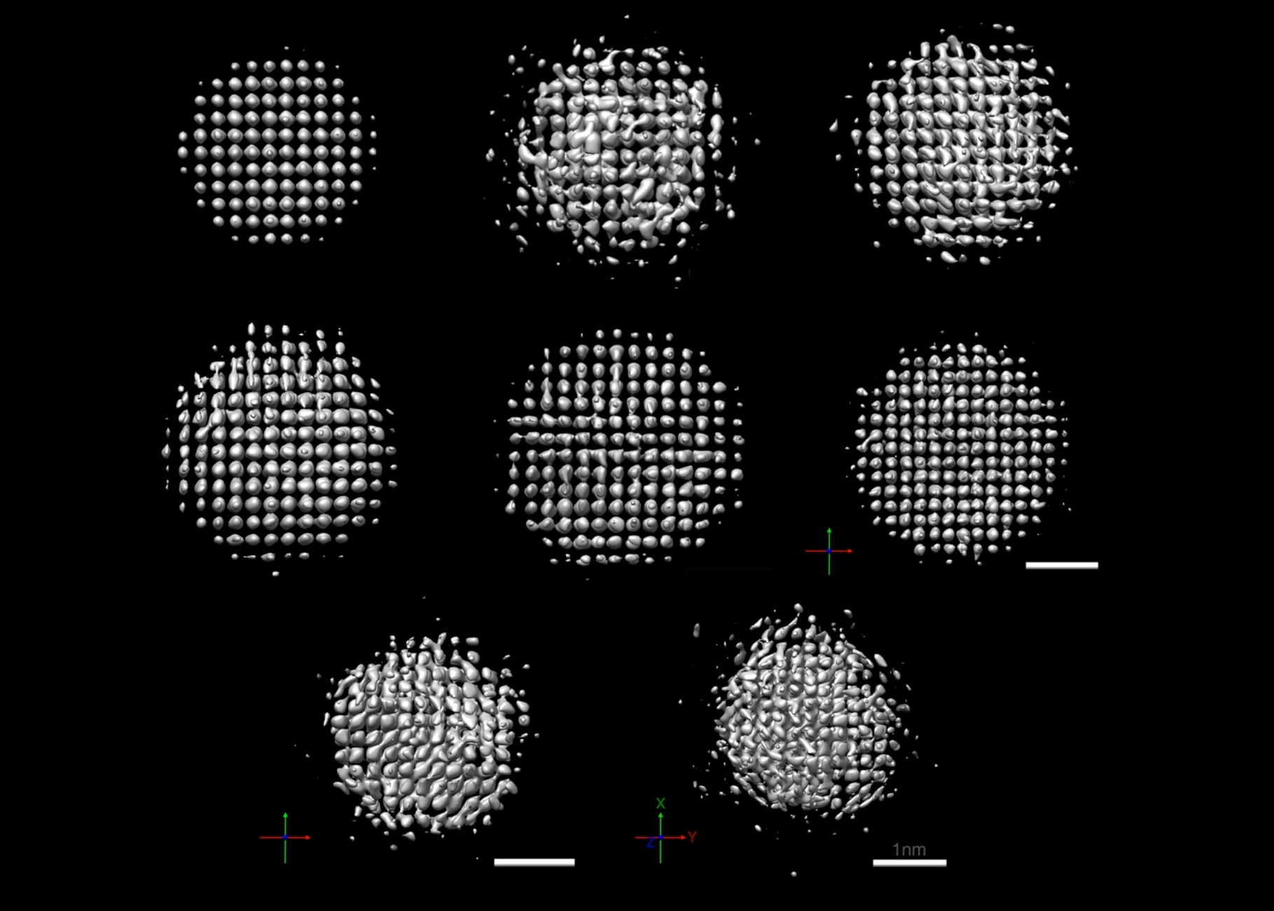
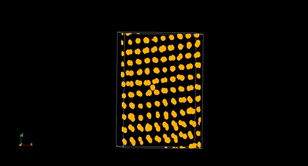
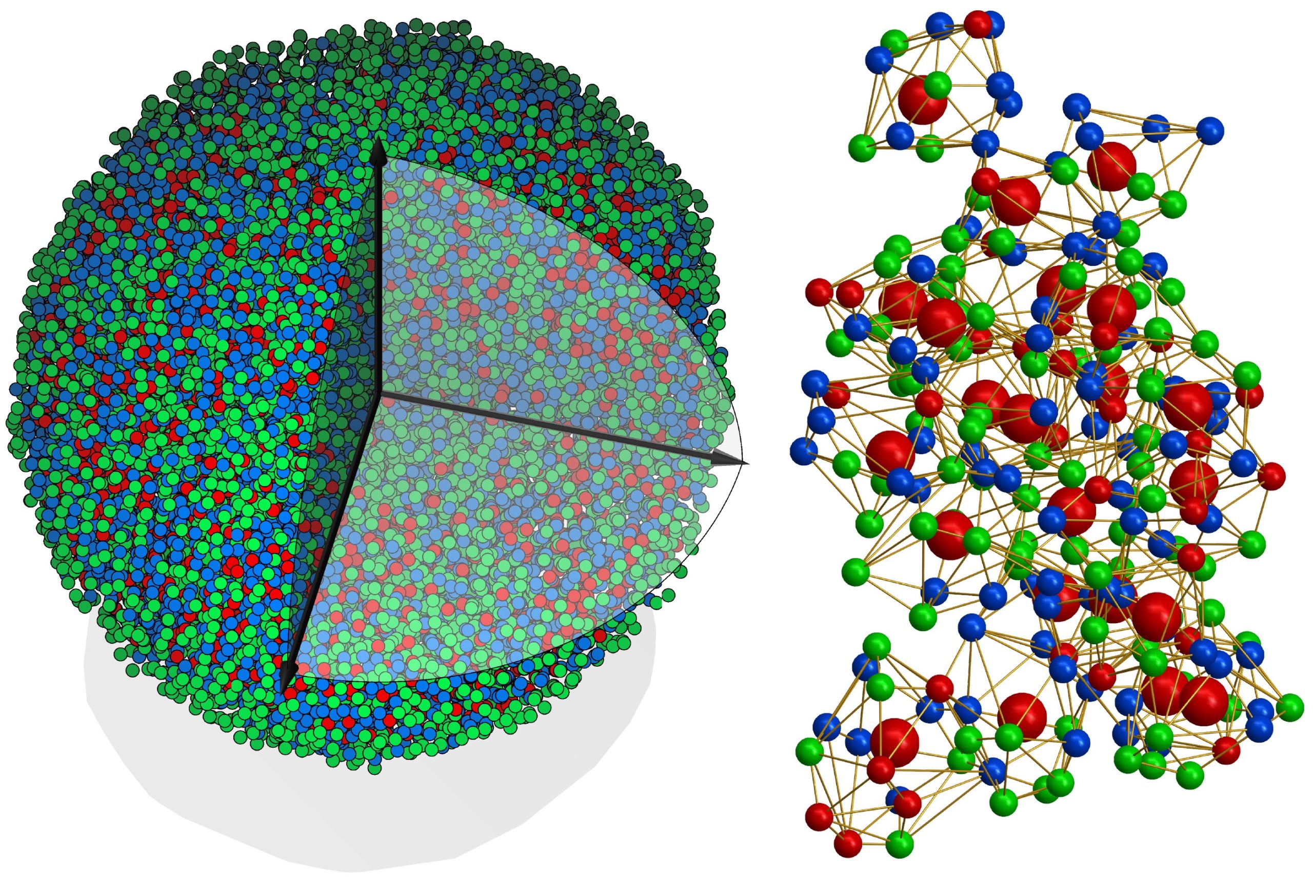
Century-Old Problem Solved With First-Ever 3D Atomic Imaging of an Amorphous Solid
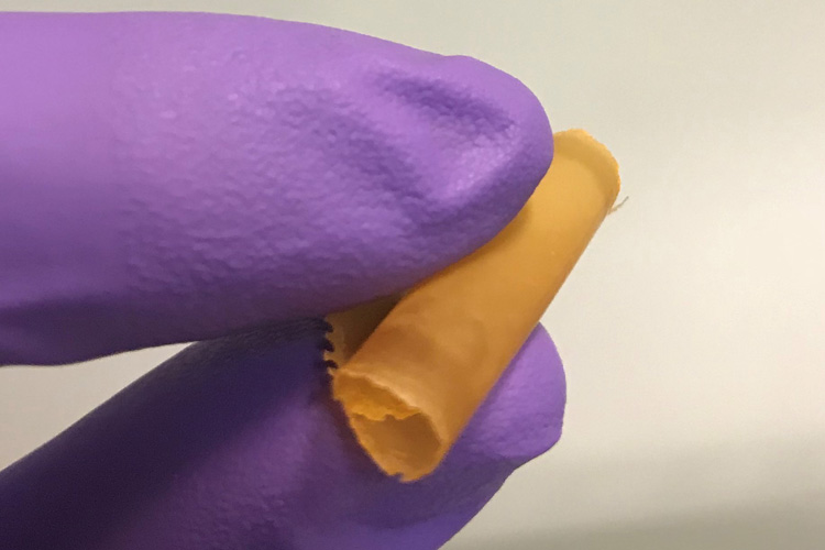
This Ultrathin Sensor Could Save Your Lungs – and the Climate

Shine On: Avalanching Nanoparticles Break Barriers to Imaging Cells in Real Time

9 Berkeley Lab Scientists Named 2020 AAAS Fellows

What’s Nanotechnology? Kristin Persson Explains at 4 Different Levels

2D Electronics Get an Atomic Tuneup
Paul Alivisatos Wins Priestley Award

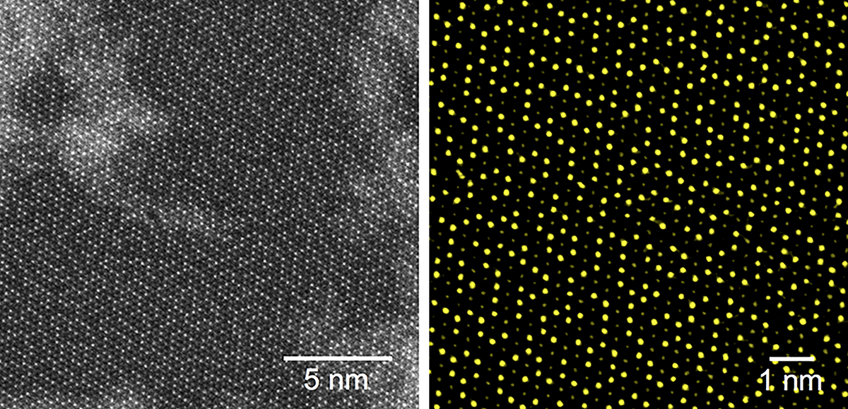
Scientists Capture 3D Images of Nanoparticles, Atom by Atom, With Unprecedented Precision