Key Takeaways
- Berkeley Lab scientists showed a novel way to build advanced transistors decades before similar structures reached smartphones.
- Their bottom-up approach crafted transistors at 2-nanometer scale through chemical synthesis.
- As smartphone chips shrink ever smaller, this pioneering approach could help solve tomorrow’s manufacturing challenges.
As the microelectronics industry moves to adopt gate-all-around transistor designs in next-generation smartphones, groundbreaking research from nearly 20 years ago at Lawrence Berkeley National Laboratory (Berkeley Lab) demonstrated an innovative approach to creating these advanced structures.
The technology – called gate-all-around field-effect transistors (GAA-FET) – represents a key architectural advance for packing billions more transistors into the tiny microchips that are found in smartphones and laptops. The “gate-all-around” design enhances control over the transistor channel, leading to better performance and lower power consumption. While industry is now implementing GAA-FET through traditional top-down fabrication, Berkeley Lab’s early bottom-up approach showed the potential of this geometry using chemical synthesis to achieve these complex structures.

In the gate-all-around (GAA) structure (at right), a gate surrounds all four sides of nanoscopic silicon channels shown as three gray nanowires intersecting a golden rectangle. These channels are passages for current flows. In the fin field-effect-transistor (FinFET) structure (left), a gate covers just three sides of a rectangular channel shown in gray. The GAA structure can control current flows more precisely. (Credit: Yu Shan/Berkeley Lab)
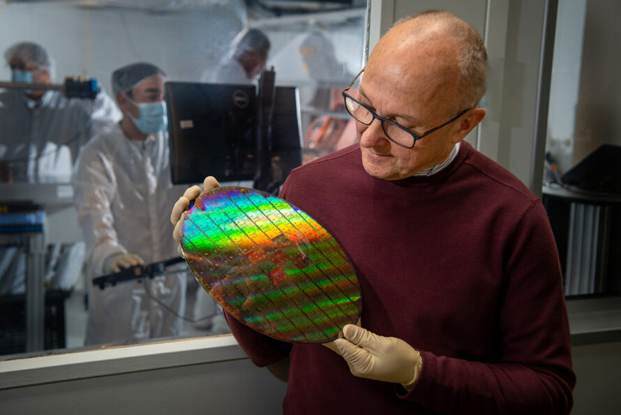
“I’m pleased to see the continued evolution of transistor architectures in the semiconductor industry,” said Peidong Yang, who published work on bottom-up synthesis of gate-all-around structures in a pioneering paper in 2006. “Our early exploration of chemical synthesis approaches to creating complex transistor geometries demonstrated alternative pathways for fabricating these structures.” Yang is a faculty senior scientist in Berkeley Lab’s Materials Sciences Division and a professor of chemistry and materials science and engineering at UC Berkeley.
Transistors are the fundamental building blocks of modern computing – and some of the best-performing microchips in smartphones today consist of more than 10 billion of them, each just 5 nanometers in size. Each transistor acts like a switch, allowing or blocking the flow of current through a semiconductor channel, enabling the binary operations that underpin modern computing.
A transistor’s gate is the control input that determines whether the transistor is on or off. For the past decade, the most common transistor design was the FinFET (Fin Field-Effect Transistor), which positioned the semiconductor channel vertically, like a fin on a tiny surfboard, with the gate wrapping around it on three sides. Shrinking the FinFET below 5 nanometers, however, reduces gating and energy efficiency.
Microchip manufacturers want to continue pushing the limits of Moore’s Law by packing tens of billions more transistors into a chip no bigger than the size of a fingernail. A higher transistor density would require even smaller transistors – down to 2 nanometers (the size of a DNA strand) or, more ambitiously, the size of a few silicon atoms (1 nanometer). Smaller chips means smaller devices and can also make chips more energy-efficient.
The microelectronics industry has known for decades that the gate-all-around approach – a design concept that wraps the gate all the way around the channel – could potentially make a higher-performing, more efficient transistor at sub-5-nanometer scales. While traditional top-down lithography faced technical challenges in fabricating GAA-FET geometries in the early 2000s, researchers were exploring various approaches and structures to realize this design concept.
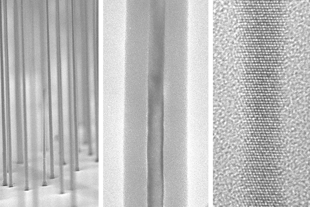
In a scientific first, the Yang group demonstrated an unconventional bottom-up approach to creating silicon-based, gate-all-around transistors using chemical vapor deposition (CVD). In their seminal 2006 paper in Nano Letters, “Silicon Vertically Integrated Nanowire Field Effect Transistors,” Yang and team used CVD to grow vertical silicon nanowires coated with an ultrathin metallic layer and embedded in silicon dioxide. This achieved a gate-all-around structure using industry-standard materials, but through chemical synthesis rather than traditional lithography.
The device properties of these bottom-up silicon-nanowire transistors rivaled those of standard transistors at the time. In recent years, microchip manufacturers have moved to embrace the gate-all-around concept, achieving the architecture through top-down fabrication approaches.
“It’s fascinating to see how semiconductor technology has evolved over the past two decades,” Yang said. “Our early work exploring different approaches to transistor design was part of the broader research community’s efforts to advance microelectronics.”
Yang’s work demonstrated the fundamental viability of the GAA-FET architecture when many in the field considered it merely theoretical. By successfully creating functional gate-all-around structures through CVD, the Berkeley Lab team validated the superior electrostatic control that would later become the primary motivation for industry adoption. This early proof-of-concept work helped establish that complete gate wrapping could indeed deliver the performance improvements that theory predicted, providing confidence for the substantial R&D investments that followed.
###
Lawrence Berkeley National Laboratory (Berkeley Lab) is committed to groundbreaking research focused on discovery science and solutions for abundant and reliable energy supplies. The lab’s expertise spans materials, chemistry, physics, biology, earth and environmental science, mathematics, and computing. Researchers from around the world rely on the lab’s world-class scientific facilities for their own pioneering research. Founded in 1931 on the belief that the biggest problems are best addressed by teams, Berkeley Lab and its scientists have been recognized with 16 Nobel Prizes. Berkeley Lab is a multiprogram national laboratory managed by the University of California for the U.S. Department of Energy’s Office of Science.
DOE’s Office of Science is the single largest supporter of basic research in the physical sciences in the United States, and is working to address some of the most pressing challenges of our time. For more information, please visit energy.gov/science.
Compute This: Six Ways Berkeley Lab is Shaping the Future of Microelectronics
Science Power-up: The Most Exciting Thing in Microelectronics