
All News

Berkeley Lab’s Big Science Stories of 2025

An image of nine panels showing either laboratory sciences, science figures, astronomical scenes, and colored blocks.

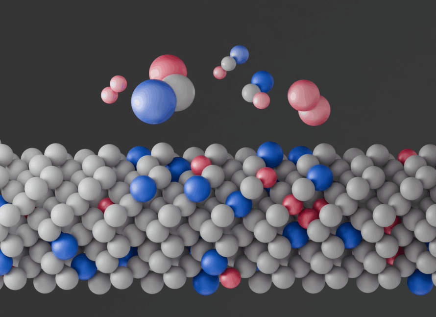
Atomic Neighborhoods in Semiconductors Provide New Avenue for Designing Microelectronics

An illustration showing a layer of closely packed spheres, mostly gray, with a few blue and red ones mixed in. Floating above the layer are several small clusters of spheres in different arrangements of the blue, red, and gray.

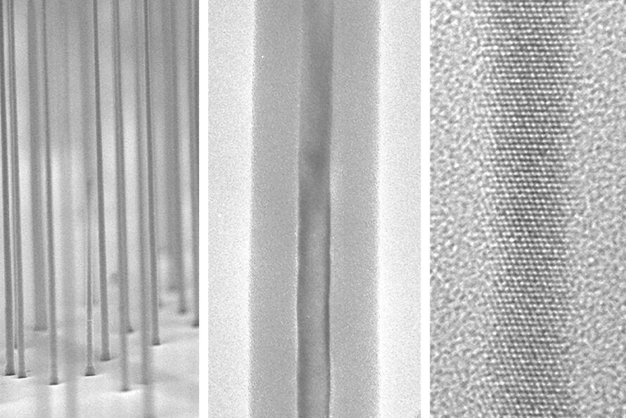
Early Research Demonstrated Novel Approach to Next-Generation Transistor Design

Electron microscope images

Science Power-up: The Most Exciting Thing in Microelectronics

A man wearing a burgundy sweater, light-blue button-down shirt, and dark-rimmed eyeglasses stands in front of machinery made of transparent and black-toned materials while holding a large, rainbow-colored reflective disc in a clean room setting with white walls.

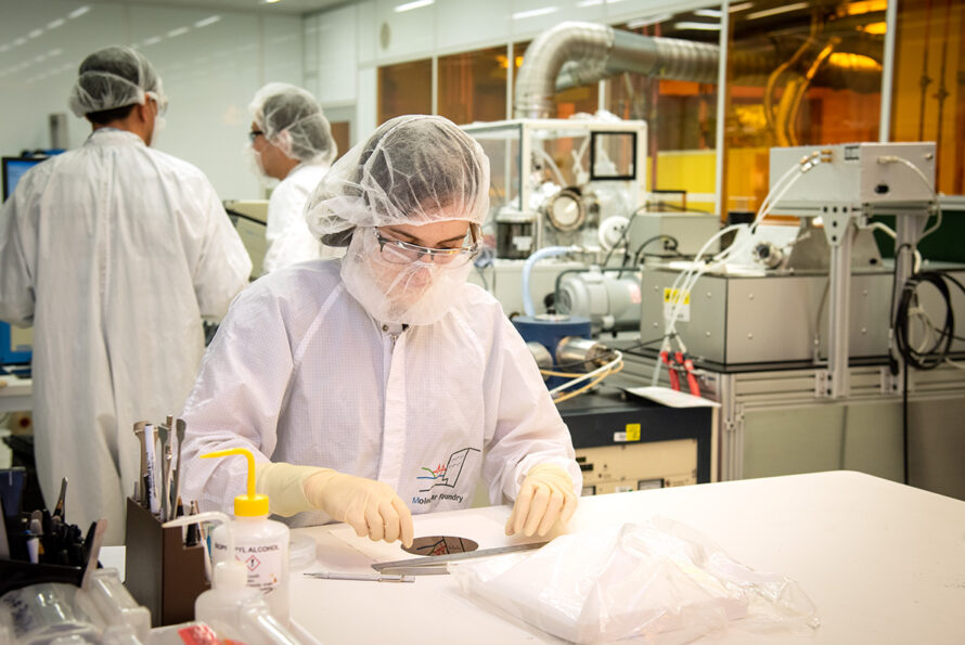
Six Scientific Advances Made Possible by Berkeley Lab’s Molecular Foundry

A clean room with employees working at workstations on the left, a work table in the center with an employee looking down at a sample.

Bringing Discoveries to Light: Six Ways the Advanced Light Source Is Accelerating Technology Breakthroughs for Society

The Advanced Light Source dome as seen from an aerial drone at sunset looking towards the San Francisco Bay and Golden Gate Bridge.

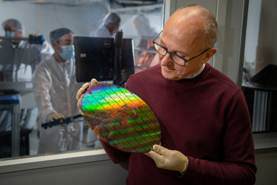
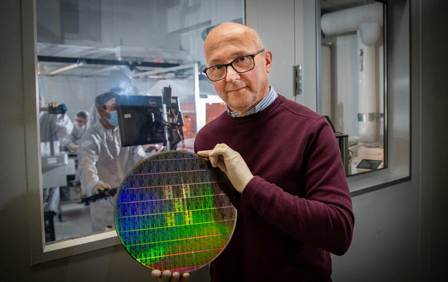
Expert Interview: Bruno La Fontaine on Chip Manufacturing Advances at the ALS

Bruno La Fontaine, Director of the Center for X-ray Optics (CXRO), speaks on how the CXRO supports the microchip industry.

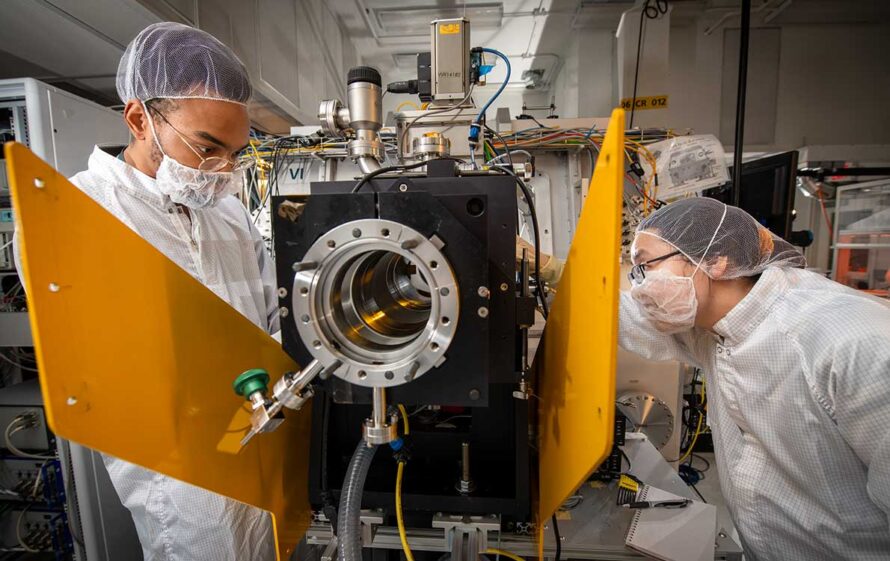
Compute This: Six Ways Berkeley Lab is Shaping the Future of Microelectronics

Two researchers donning personal protective equipment inspect a mirror chamber used to create custom and dynamic illumination patterns for testing the limits of semiconductor materials.

New Photon-Avalanching Nanoparticles Could Enable Next-Generation Optical Computers

Scientist in protective eyewear adjusts a microscope in a high-tech lab filled with optical and electronic equipment.

A New Approach to Efficient Optoelectronics, Inspired by the Human Eye

A recipe for energy efficiency: an optical sensor that also processes data. The transparent dome represents interactions between photons (red and green) and the nanoscale elements on the substrate. Carbon nanotubes with quantum dots (small spheres) are shown connected to CMOS circuitry below.

Scientists Capture Images of Electron Molecular Crystals

2 rows of 3 scanning tunnel microscope images showing purple shapes against a dark background.

Researchers Succeed in Taking 3D X-ray Images of a Skyrmion

A rendering in paraview of the product of the 3D reconstruction. (Credit: David Raftrey)