Tag: materials sciences
Electron Microscopy Reveals New Method to Make Exotic Metal Alloys
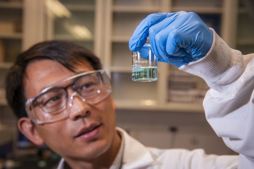
New Process Uses Microbes to Create Valuable Materials from Urine

Computational Chemistry Unlocked: A Record-Breaking Dataset to Train AI Models has Launched

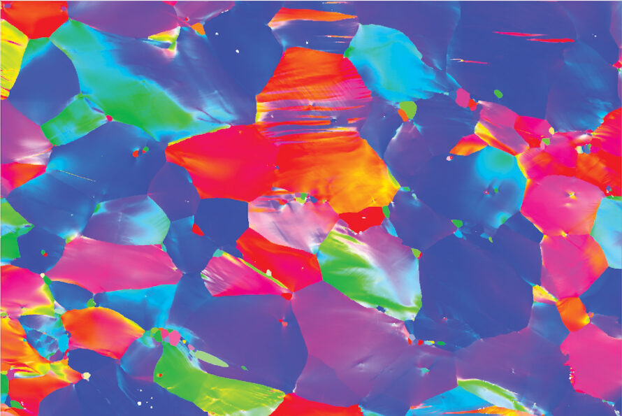
This Alloy is Kinky
How X-Rays Can Make Better Batteries

Scientists Discover ‘Secret Sauce’ Behind Exotic Properties of New Quantum Material

With a Little Help, New Optical Material Assembles Itself

Technique Tunes Into Graphene Nanoribbons’ Electronic Potential

New Smart-Roof Coating Enables Year-Round Energy Savings

These Tiny Liquid Robots Never Run Out of Juice as Long as They Have Food

How Can Next-Gen Computer Chips Reduce Our Carbon Footprint?

Physicists Snap First Image of an ‘Electron Ice’